How to Panelize PCBs within KiCad

Learn to panelize PCBs entirely in KiCad with key footprints and techniques for optimal fabrication and minimal warpage in assembly.
By
Kyle Hunter
June 25, 2025
 (Updated
August 2, 2025
)

Panelizing PCBs from withing KiCad

I’ve posted two YouTube videos (Video 1 & Video 2) going over how we panelize PCBs entirely with KiCad. In doing so, we use several footprints I created. The most important two are the SINGLED_SIDED_TAB and the DOUBLE_SIDED_TAB. These footprints use the Cmts.User layer to show the fab house where a 2mm router should be used. The panel below was DFM'd and rendered using the gerber tool Fab3000.
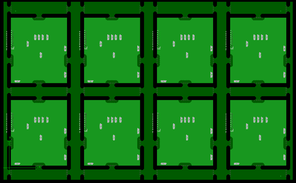
Example of PCB panel created within KiCad
Render of a mouse bite tab created within KiCad using our library. Notice the large supports going North and South. This ensures that your assembly house will not have to battle panel warpage while assembling.

The biggest drawback of using KiCad like this is that there is no way to directly update the panel when the PCB version updates. Our method focuses on making the initial panel as simple/fast as possible. When needing to update the board, it is quick enough to just recreate the entire panel directly. One item to note that I don’t fully mention in the video is in regards to the Cmts.User. You must ensure that no other footprint on the board uses this layer. Some default KiCad mounting holes use it. This can make the fab house upset and potentially make a mistake on the creation of the board.

The Github link to our panelizing library can be found here.

Need help with PCB design or panelization for production? MicroType Engineering offers PCB design services and PCB assembly from prototype through production volumes. Contact us to get started.

Recent Blogs

Securing the Future: Our Commitment to ITAR and CMMC Compliance
Created at:  
June 25, 2025
Updated at:  
August 2, 2025
Kyle Hunter
Open cardboard box with flaps folded outward, icon style.
Uncatogrized
Chat bubble icon representing comments or messaging.
Comments
White heart icon on transparent background.
0
Explore ITAR, NIST 800-171, and CMMC compliance to secure defense and aerospace projects. Trust MicroType Engineering for advanced data security solutions.
KiCad 9 Jobsets: Automating Your Design Outputs
Created at:  
January 4, 2026
Updated at:  
January 22, 2026
Kyle Hunter
Open cardboard box with flaps folded outward, icon style.
Uncatogrized
Chat bubble icon representing comments or messaging.
Comments
White heart icon on transparent background.
0
Standardize your KiCad workflow with jobsets. Configure automated exports for Gerbers, BOMs, renders, and more with a single click
MOSFET Selection Guide: Rds(on), Vgs, and What Actually Matters
Created at:  
June 25, 2025
Updated at:  
September 11, 2025
Kyle Hunter
Open cardboard box with flaps folded outward, icon style.
Uncatogrized
Chat bubble icon representing comments or messaging.
Comments
White heart icon on transparent background.
0
Learn a practical approach to selecting the right MOSFET for various applications. Discover how to filter options effectively for low and high-power needs.
Buck Regulator Design For Conducted Emissions
Created at:  
June 25, 2025
Updated at:  
August 2, 2025
Kyle Hunter
Open cardboard box with flaps folded outward, icon style.
Uncatogrized
Chat bubble icon representing comments or messaging.
Comments
White heart icon on transparent background.
0
Discover the importance of conducted emissions testing for DC lines and how buck converters impact compliance. Learn effective filtering strategies here.

MicroType Engineering strives to help businesses turn an idea into a physical product. Whether you are already established and seeking to branch out into a new product or working on an exciting new startup project, MTE can guide you along the way.

MTE provides rapid prototyping, enabling you to quickly have a physical product in your hands to showcase and test. MTE offers a personalized approach, helping navigate the often confusing, and expensive path to manufacturing and selling a product. Contact us to learn more.