
Protecting Circuit Board Power Inputs from Surge Events
Introduction
In past posts, I have gone over TVS diodes and general input protection for power supplies. What I have not shown until now is a direct simulation of how different protection schemes behave during a surge test.
In this article, I use the Falstad circuit simulator to recreate the IEC 61000-4-5 surge waveform and then apply it to a simple circuit board input. The goal is not to create a perfectly accurate quantitative model, but rather to compare different protection strategies side by side in a qualitative way. This is meant to be a brief overview of common approaches rather than an in-depth dive into any single protection method.
The Surge Waveform
The IEC 61000-4-5 standard defines the surge waveform in two conditions:
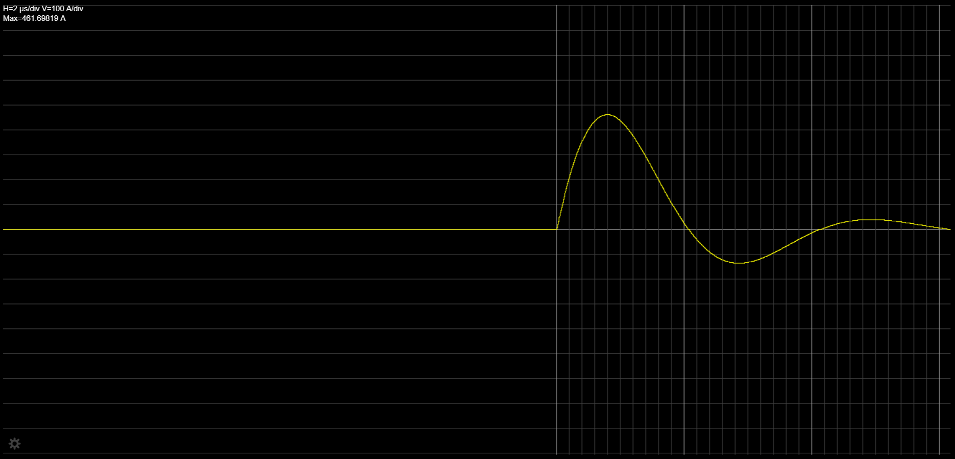
- Open-circuit voltage: 1.2 µs rise, 50 µs decay
- Short-circuit current: 8 µs rise, 20 µs decay
For this article, I am simulating a 1 kV surge level, which corresponds to Class 2 in the standard. Class 2 represents environments where cables are reasonably well separated but still subject to parallel routing with power and signal lines. Higher test levels such as Class 3 (2 kV) or Class 4 (4 kV) are used for harsher electrical environments, but Class 2 is a common baseline for many circuit boards.
In Falstad, I built a simplified generator circuit with blocking diodes to prevent ringing. This gives a good baseline for comparing protection schemes.

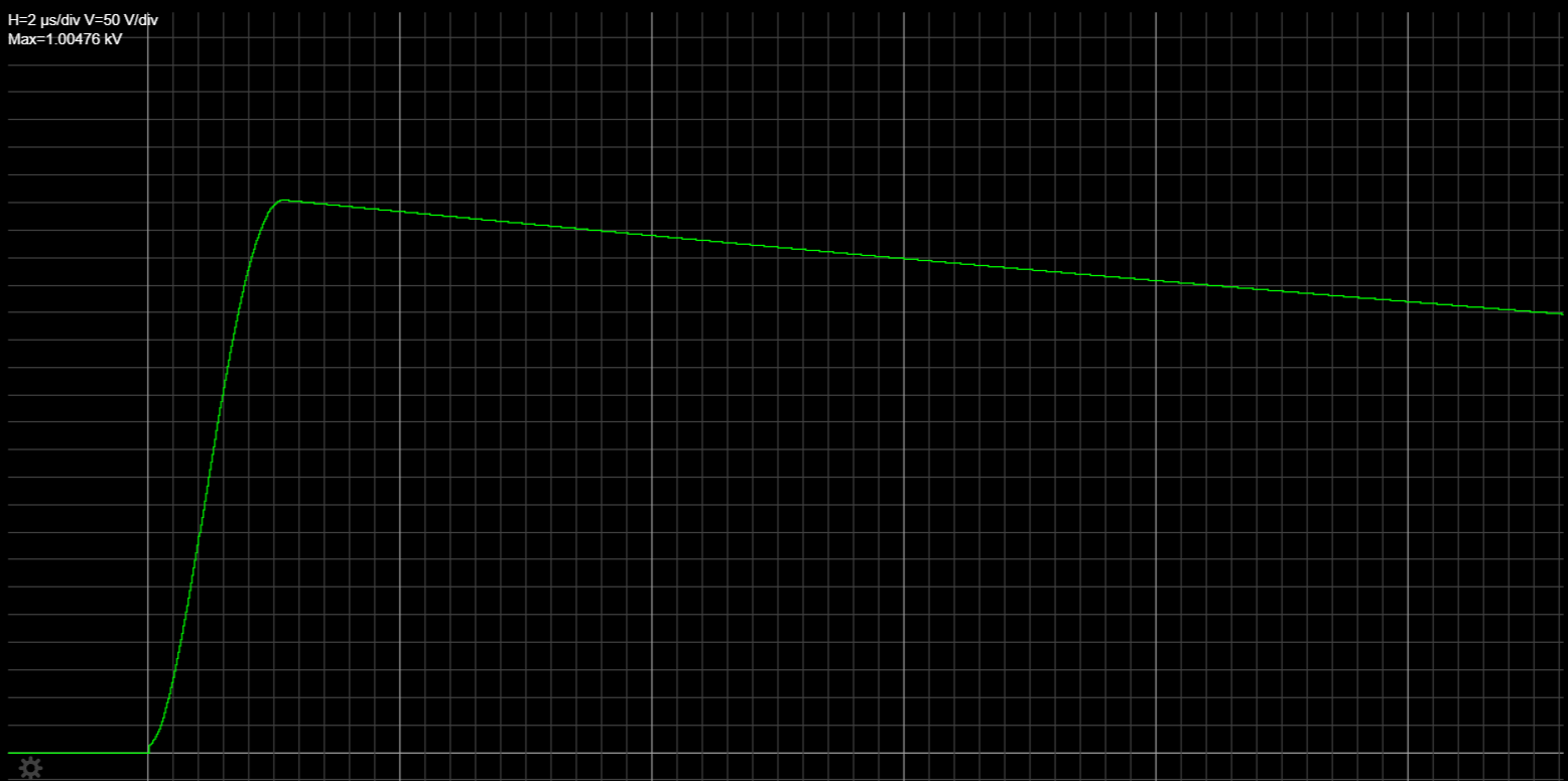
To validate the setup, the simulation output roughly matches the expected IEC waveforms. The plot below shows the open-circuit voltage (1.2/50 µs) and the short-circuit current (8/20 µs) from the generator circuit.

Test Setup
Before looking at the different protection elements, it is important to explain the full test setup used in the simulations. The surge generator itself was built to follow the IEC 61000-4-5 standard and was described earlier. To make the results meaningful, I also needed a simple but representative load circuit to act as the “device under test.”
In the simulation, the surge generator connects to a 12 V supply rail that feeds into a basic circuit board input stage. The setup includes:
- 12 V DC source to represent the system supply voltage
- 10 mΩ series resistance to model trace and wiring parasitics
- 2 µF capacitor across the input as a stand-in for bulk decoupling and general board capacitance
- 220 Ω resistor as a load, simulating a circuit drawing a modest amount of current
- Optional components (electrolytic capacitor, TVS diode, series resistor, or gas discharge tube) that are added one at a time to show their effect
This simplified DUT is not intended to perfectly replicate any single product, but it provides a realistic way to see how surge energy interacts with common input components.
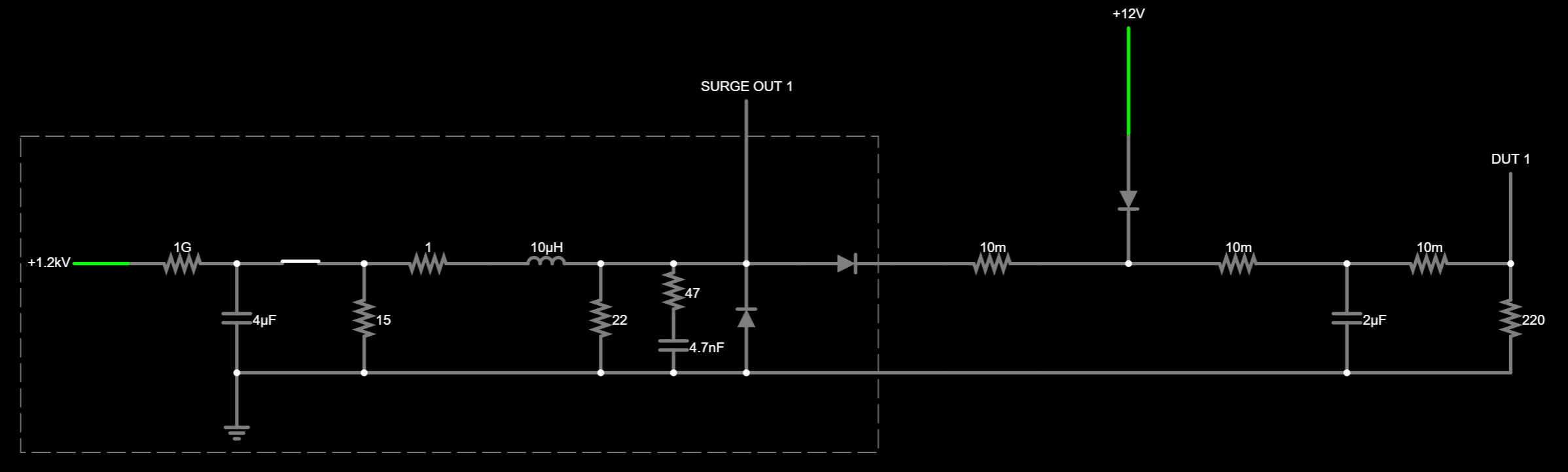
By starting with this baseline circuit and then adding protection elements one at a time, it becomes much clearer how each device changes the surge response.
No Protection
The first case is with no protection at all. The surge generator connects directly to the board input and the result is exactly what you would expect.
- The full 1 kV surge appears across the input.
- The voltage lingers since it has no discharge path.
- In a real circuit this energy would arc through components or traces.
While there would normally be some leakage paths such as PCB surface resistance or component leakage, the simplified model without them is fine for demonstration purposes.
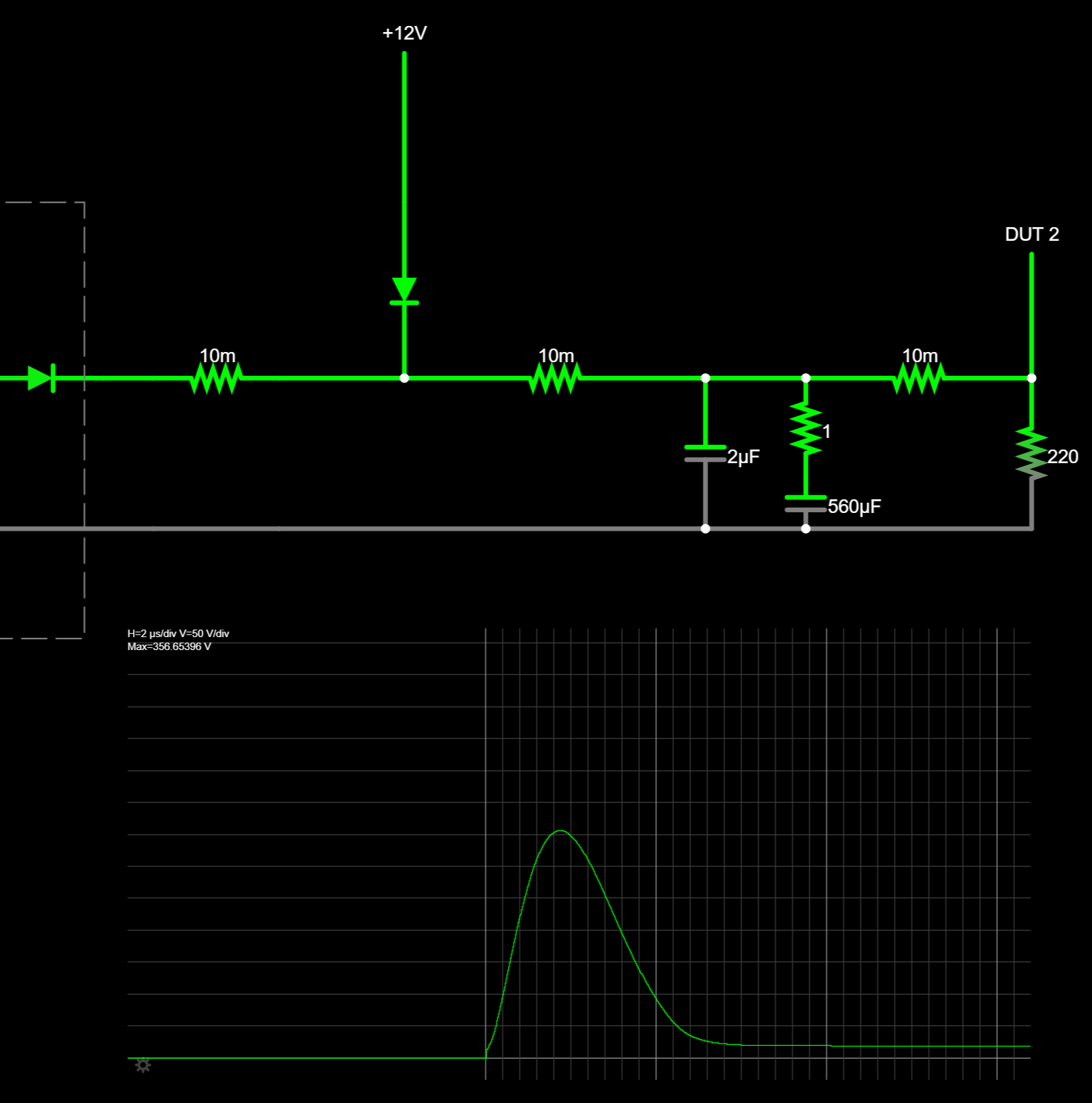
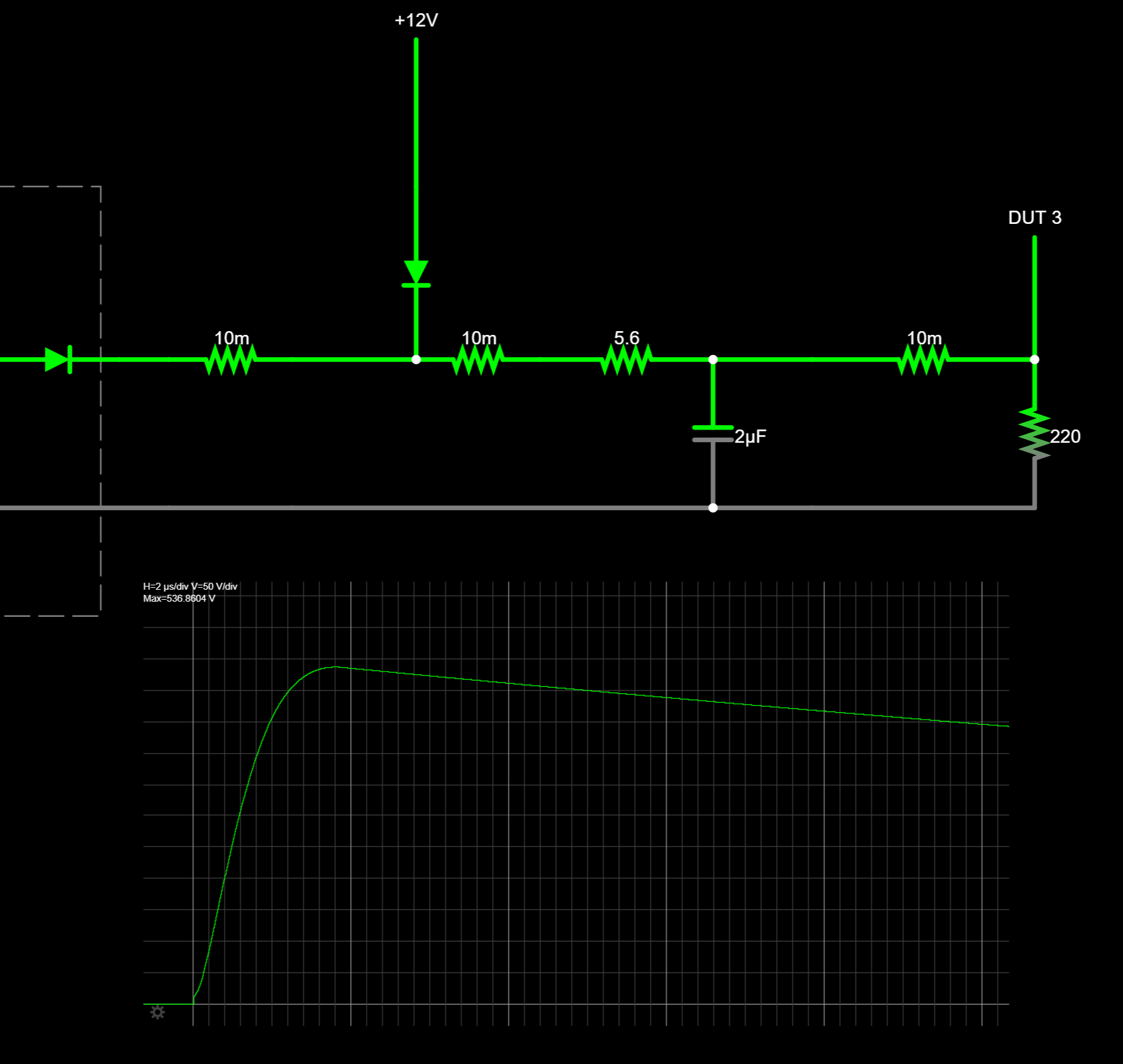
Bulk Capacitance
Adding a large electrolytic capacitor makes a major difference. In this case I used a 560 µF capacitor with a small series resistance to represent ESR.
- Peak voltage drops to about 356 V.
- The decay is faster since the capacitor absorbs energy.
- The capacitor dissipates several kilowatts of peak power, which may damage it if used alone.
For background on capacitor (ceramics specifically) behavior under a DC voltage, see my article on DC Bias Effect in Ceramic Capacitors.
Series Element: Resistor or Inductor
A simple series resistor (or inductor) can slow the rise of the surge. In the simulation, the rise time stretches from about 1 µs to 15 µs.
- Lower rise time means less surge energy.
- The resistor must be chosen carefully so it does not limit normal operation.
- An inductor can provide the same benefit without dissipating steady-state power, but the saturation current is critical. The inductor must be sized so it does not saturate during the surge.
For a deeper look at how series resistors improve signal integrity and EMC, see my earlier article on rise time and series resistors.
Need an IEC 61000-4-5 review?
We provide surge and EFT pre-compliance testing plus redesign support.
Contact us to learn more about our EMC & Pre-Compliance Testing services
TVS Diode
TVS diodes are specifically designed to clamp surge events. In the simulation, a 15 V part limits the surge to about 37 V at the input.
- Voltage downstream is now in a survivable range.
- The diode dissipates almost 7 kW of peak power for tens of microseconds. Datasheets specify ratings under these short surge pulses, and parts must be selected accordingly.
- In practice, multiple devices or additional elements are typically needed.

Gas Discharge Tube
Gas discharge tubes (GDTs), sometimes called lightning protection tubes, are ceramic devices filled with inert gas. When a surge exceeds their breakdown voltage, the gas ionizes and creates a low resistance path, safely discharging the current away from sensitive circuits. They can handle very high surge currents and have extremely high insulation resistance during normal operation.
Key points about GDTs:
- Very high surge current capability and low leakage in normal conditions.
- A big gotcha is the follow current problem. Once triggered, the tube may stay latched on if the supply voltage is higher than its arc voltage.
- To prevent this, GDTs are usually paired with a TVS diode, MOV, or series element so they release after the surge.
- Selection must account for both the DC spark-over voltage (above the circuit’s normal maximum voltage) and the impulse breakdown voltage at fast surge rise times.
- Due to their relatively high on resistance and capacitance, they typically respond too slowly to be a standalone protection device.

GDT vs TVS vs MOV
Gas Discharge Tubes (GDTs) are best for high-energy, slower surges like lightning. They can handle kiloamps, but their response time is in the hundreds of nanoseconds, and they may stay latched without a series element.
Transient Voltage Suppressors (TVS diodes) react in picoseconds and are ideal for protecting sensitive ICs, but they have limited surge current and must be sized carefully. The quoted “7 kW” in the simulation is a peak pulse for tens of microseconds; datasheets specify peak pulse power ratings under these same test pulses.
Metal Oxide Varistors (MOVs) fill the gap. They absorb repeated surge events and are common at mains inputs. Unlike GDTs, they don’t latch, but unlike TVSs, they degrade over repeated hits. In practice, MOVs are often used at the AC input, followed by GDT + TVS near the load for multi-stage protection. For a deeper dive, see Designing ESD Protection Circuits.
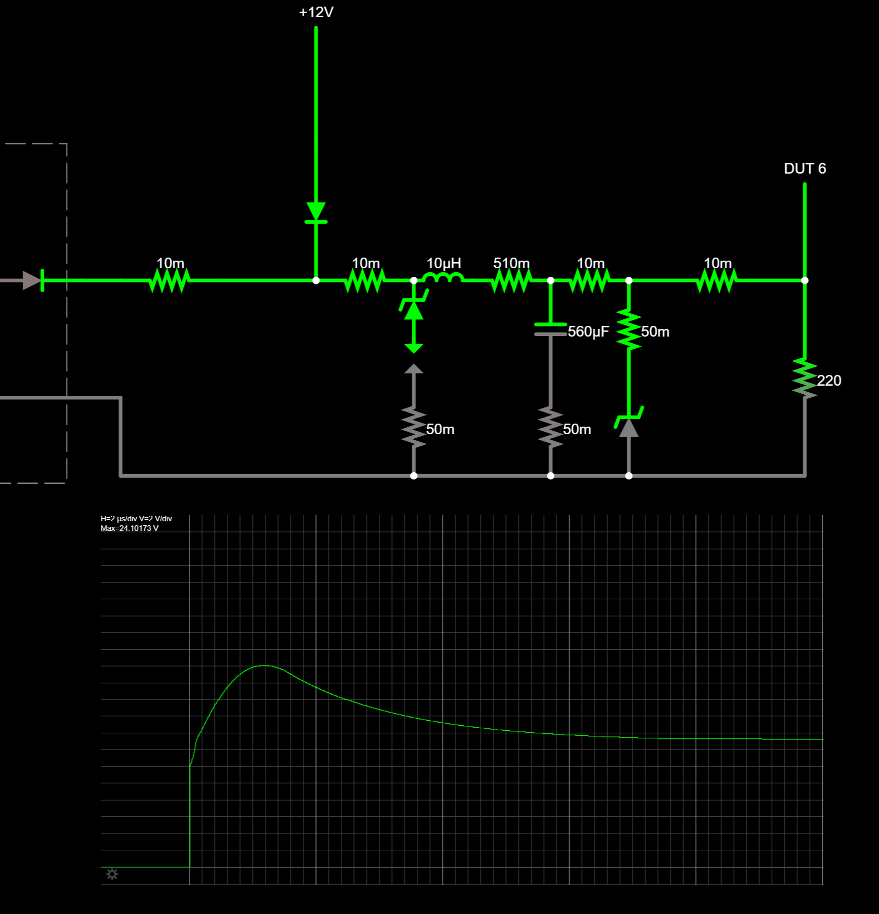
Combined Approach
The most effective method is layered protection. By combining several elements, each device handles only part of the surge energy.
The example below uses:
- Gas discharge tube to absorb the largest part of the surge
- Series resistor (or inductor) to slow the rise
- Electrolytic capacitor to provide a discharge path and help absorb energy
- TVS diode to clamp the residual voltage
The result is a robust protection network:
- Input voltage clamped to around 24 V
- TVS diode peak power reduced to less than 3 kW
- GDT current limited to about 50 A, well within typical ratings
Comparison Table
Need surge protection designed into your board? Contact us for a design review.
Next Steps
This article focused on the basics of surge suppression using simple passive components. In a real design you might also add:
- π filters to reduce ringing and noise, especially effective for conducted emissions.
- MOVs for AC mains input protection or anticipated surges beyond what a TVS can handle.
- eFuses with back-to-back MOSFETs for disconnect during extreme events.
For background on eFuses and how they combine multiple protection types, see PCB Power Input Protection.
You can also find more about board-level design strategies in our posts on panelization in KiCad and assembly line upgrades, since proper production planning goes hand-in-hand with robust input protection.
Conclusion
Surge events are among the most destructive tests a circuit board can face. By layering multiple protection devices, you can ensure that your board survives and continues to function.
At MicroType Engineering we design and test industrial controllers, aerospace systems, and high-reliability electronics that must meet IEC surge and EMC standards. If you need help protecting your product, reach out to us. Learn more about our electronics design services.
FAQ
Q: What is IEC 61000-4-5?
A surge immunity standard defining waveforms and test levels for electronic equipment.
Q: Can a TVS diode alone protect against surges?
It clamps voltage but may fail if forced to dissipate too much energy. Layering with other elements is safer.
Q: Should I use MOVs on low-voltage DC inputs?
Generally no. MOVs are more suited for AC mains. TVS diodes and capacitors are preferred for DC.
Q: What’s the difference between surge and ESD protection?
Surges are long, high-energy events (µs to ms). ESD is a fast, lower-energy discharge (ns). Circuits must be designed for both.


.webp)