
A Pragmatic Approach to Selecting a MOSFET
The target for this post is to be a sort of follow up to my original power MOSFET post. While the goal of the prior post was to “de-mystify” issues surrounding MOSFETs, this will put that info into practice. I will outline several important considerations when selecting a MOSFET for a particular application. I will be using three common scenarios in circuit design for the basis of the MOSFET selection. Then I will show a practical approach for filtering down parts, until a selection of parts remain, all of which will work.
For all searches I like to use DigiKey, as I feel that they have a slightly better search function than others.
Scenario 1: Selecting a Low-power indicator/buzzer MOSFET
A common application for MOSFETs in nearly every practical circuit is to drive indicator LEDs. It is normal for a LED or buzzer to draw 10mA-50mA. Likely, your microcontroller of choice won’t be able to sink/source that much current on an IO pin. Or, even if it can, you want to avoid pushing it to its limit. This is where a logic-level MOSFET comes in handy.
For a deeper dive into LED driving strategies, check out our article on advanced LED driver circuit design.
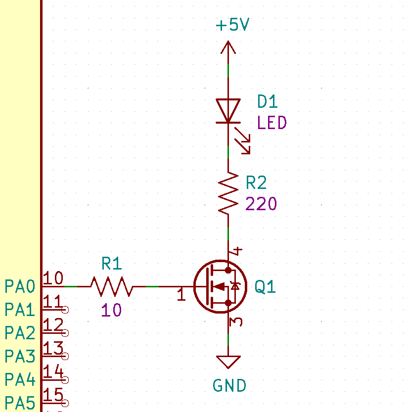
- Max current from drain to source ~ >500mA (this spec is loose)
- Max voltage from drain to source > 12V
- Voltage drive on gate 3v3.
The criteria for this MOSFET is quite lenient, with the most aggressive spec being that it needs to be directly driven from 3v3 logic. Most microcontrollers will output at 3v3 logic with the exception of AVR and some older series of Microchip lines.

Narrowing down the search
The first step is to start up a new Digikey search for MOSFETs. With no filters on, there are over 40,000 different parts! My primary goal is to eliminate as many parts that don’t fit the criteria as soon as possible, to make further filtering easier. I filter In stock, Cut Tape (CT), Active, N-Type, and MOSFET (Metal Oxide). That instantly limits the search to 3,675 parts.
The only filter that potentially filters parts too aggressively is the Cut Tape (CT) parameter. The reason for that filter is to eliminate duplicate SMT parts that use different packaging. Some through hole parts are only sold exclusively on Bag, Box, and Bulk. Since this scenario I only care about surface mount parts, that doesn’t matter. The bigger issue is the Tray and Tube. There are some SMT parts that exclusively are sold in that packaging. I really don’t care about those parts most of the time, as normally they will be older, nearly obsolete parts, or large microcontrollers. If there is an issue with me not being able to find enough MOSFETs at the end of the search, I will include them later.
The next most restrictive MOSFET selection filter is the Drive Voltage (Max Rds On, Min Rds On). This spec limits MOSFETs based on the voltage that needs to be applied to the gate to turn on the MOSFET. The Max Rds On portion is the voltage in which the MOSFET is first fully “on”. At this voltage, the MOSFET will have its largest value of Rds. The goal is to apply a voltage higher than the Min Rds On. Above this point, the Rds will be at its lowest point.
I apply a filter for:
1.2V, 2.5V
1.5V
1.8V, 2.5V
1.8V, 2.7V
2.5V
Final search criteria
We are now limited down to 9 parts! All of them have a Drain to Source Voltage (Vdss) of at least 12V. It is important to note that it is possible to use a MOSFET below the Min Rds On voltage spec. If the 9 selections aren’t enough, you can expand your search to include parts that have a Min Rds On above 3v3. Just ensure that you consult the datasheet to see the Rds value at the 3v3 gate drive voltage.
The final spec to narrow down is the Current – Continuous Drain (Id) @ 25C. I limit that with:
440mA
1.4A
2.3A
3.7A
9.3A
Now we have only 5 parts to choose from. We can select any of these MOSFETs, as they meet our specifications. From this point, to choose a specific one, it really depends on the goal of the product. For something like this, I would typically choose the cheapest option. Other than to find the correct pinout, I typically won’t dig into the datasheet, as the specs don’t affect us too much.
Scenario 2: Selecting a High-power, non-PWM’d MOSFET
Selecting a MOSFET in this scenario requires more digging and calculating. We are looking for:
- Max current of load is 20A
- Load voltage is 24VDC
- Gate voltage from driver is 12VDC
- No PWM
- No forced air convection available
This scenario is common when driving large, resistive loads like an LED array, a heater, or motor drive. We will be assuming that whatever we are driving is not inductive, and not focus on that aspect of MOSFET selection in detail.
Initial Rds equation
Before beginning a search, I like to have a rough idea of the Rds value to search for. When a MOSFET is not PWM’d, it acts just like a resistor across its drain and source. Note: the Rds is quite variable depending on temperature derating. It also may vary from specific parts within a lot. For a standard power MOSFET application without heatsinks, I like to keep the power dissipated as heat below 1W. Most standard packages are able to handle that without too much issue.
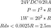
Equation 1: Power equation to find the Rds(on) at a power dissipation of 1W.
Using equation one, I find that the Rds(on) for a power of 1W, and current of 20A, is 2.5m. Using our digikey search, I start out again filtering for In stock, Cut Tape (CT), Active, N-Type, and MOSFET (Metal Oxide). We are again down to 3,675 parts.
Most restrictive filters first
The most restrictive parameter will be the Rds On (Max) @ Id, Vgs, so I filter that to include only parts equal to, or below 2.5m. We are now left with around 400 parts. The Drain to Source Voltage (Vdss) needs to be above 24VDC according to our design specs. Since this load likely will be off our board, and the wires could have an inductive component, I will give some headroom for this spec. I filter to include parts from 40V and above, leaving us just over 200 parts.
The final required spec to filter is Vgs (Max). Since we will be driving the gate with 12VDC, I only include parts at 12V above. The remaining ~200 parts all should work for our application. One spec I omitted from this search is Current – Continuous Drain (Id) @ 25°C. The reason for this, is that it can be misleading. The majority of the time, a MOSFET is limited by the heat generated due to the Rds or switching losses, not the actual continuous current rating. While you don’t want to use a part rated below our 20A, it is best to take it with a grain of salt.
Now Which MOSFET do We Select?
Next, suppose I want to only use surface mount MOSFETs, in a DPAK style package. With those last two filters, we are left with around 70 parts! That still leaves a lot of parts, all of which should work for us. The question is, which MOSFET do we select? Ultimately it will come down to your specific product, and what other criteria matters. Let’s say that cost is a major driving factor, so I sort by price, in ascending order. One of the cheapest is the TK100S04N1L,LXHQ by Toshiba Semiconductor and Storage. It is shown in Figure 3 below.
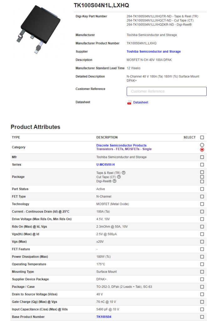
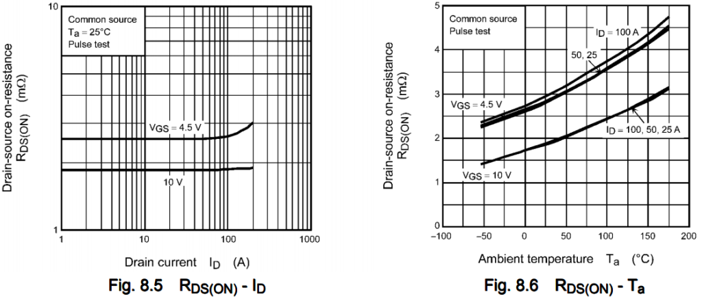
Figure 4 shows the two key charts that I will consult within the datasheet. Since we will be driving this MOSFET at 12V, we know from the above left chart that at 20A, the Rds will be around 1.9m. The right chart is derating the Rds based on the ambient temperature. For our example, we will assume this will be at ambient temperature, so no derating is required.
Fine tuning the power dissipation equation
Now that we have selected our MOSFET, and know the actual Rds value, we can fine tune our power equation. Note: I italicized “actual” above, because even when basing it on the datasheet charts, it will always be a rough approximation.
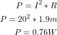
Equation 2: Power equation to find actual power dissipation based on Rds.
Using equation 2, the power that the MOSFET will dissipate as heat is 0.76W. This makes sense, as at a Rds of 2.5m, the power would be 1W. Using this 0.76W value, we can determine roughly, what the expected junction temperature of the MOSFET will be. Unfortunately, the Toshiba’s datasheet only gives us a value of Channel-to-case thermal resistance. The channel portion refers to junction, I’m not sure why they use that terminology. This spec is useful if using a heatsink, but since it doesn’t give a value for junction to ambient, we need to use a different datasheet. IPD90N04S402ATMA1 by Infineon, which is an identical package states the Thermal resistance, junction – ambient, leaded to be 62 deg k/W. Since they are the same package, we can use this spec without concern.
The equation 3 below is quite simple, and it gives us the change in temperature from ambient. It is imperative to not take this value to be the actual temperature. Assuming room temperature, 25C, the junction temperature will be 25C + 47C = 72C. While this temperature may seem high, the datasheet gives a maximum junction temperature of 175C! We are significantly below that, so I have confidence in my selection. If this 72C is too high for your application, you can repeat the search for lower Rds values, to select a MOSFET with a lower junction temperature.
Equation 3: Equation to calculate the junction temperature of the selected MOSFET.
Scenario 3: Selecting a MOSFET for High-power, PWM’d Loads
The final scenario will be the most difficult, and will require the most assumptions. The scenario is identical to the prior one, expect this load will be PWM’d. This can make a dramatic difference in how the approach to selecting a MOSFET works. Something that I omitted from my prior MOSFET post and video, is the issue of switching losses. My goal here is not to go into great detail on the topic, as there are great appnotes that discuss it like SLYT664 and AN608A While complex derivations and equations can be helpful, they often lead down a path that wastes a lot of time, and still produces inaccurate results.
Background on MOSFET Switching Losses
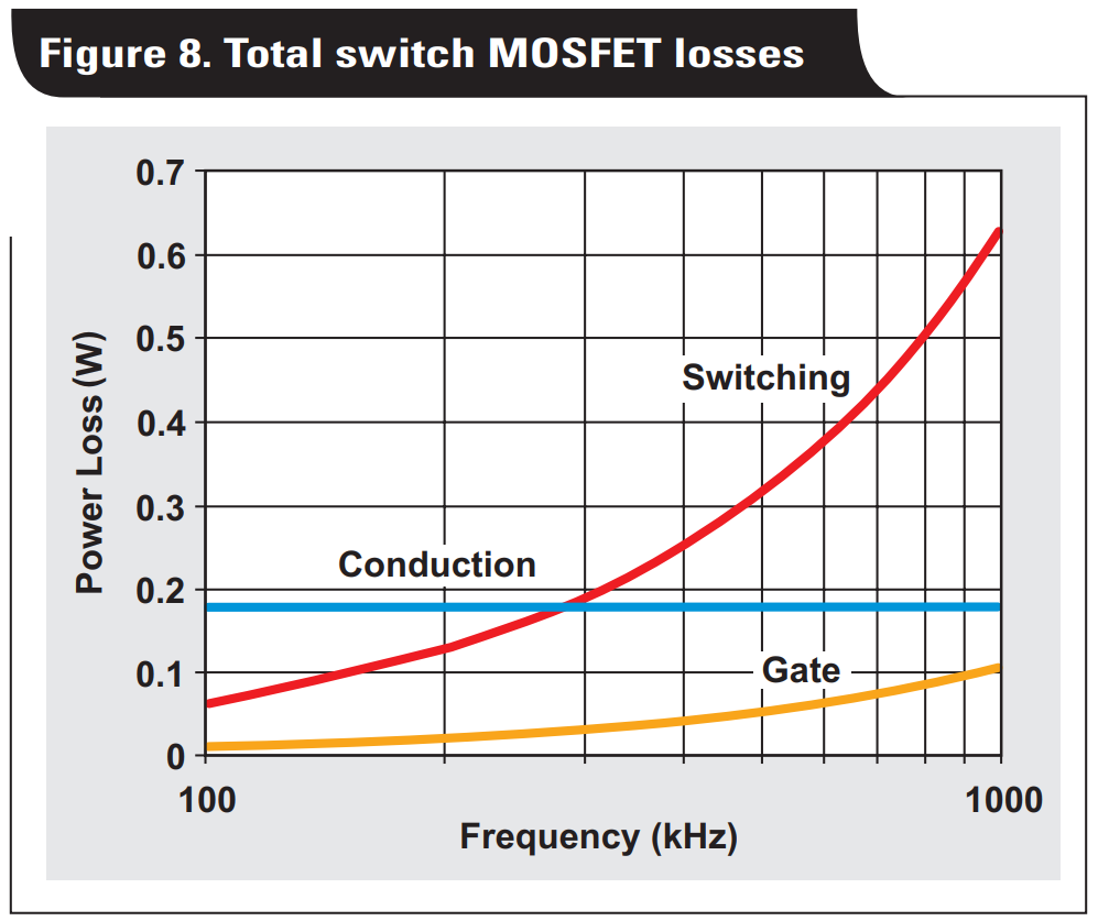
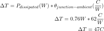
Figure 5 gives a great look at how the power is dissipated in a MOSFET depending on the frequency. Note: Ignore the actual value of the power loss, as that is MOSFET dependent. I will ignore the gate losses, as they are not significant sub MHz’s. The conduction portion of loss is simply the Rds of the MOSFET. When a MOSFET is fully on, it acts just like a resistor from drain to source. This loss does not depend on the frequency that the MOSFET is switching at. The switching loss increases rapidly with the increase of frequency.
The easiest way to think of this is:
When the MOSFET is turning on or off, the resistance across the drain to source is high. The more time spent turning on/off the MOSFET (higher frequencies), the more power is lost in that transition.
This is the core simplification that guides my methodology for choosing a MOSFET that is PWM’d.
MOSFET Selection Criteria
The criteria for this scenario is quite similar to scenario 2 with the exception of item 4:
- Max current of load is 20A
- Load voltage is 24VDC
- Gate voltage from driver is 12VDC
- PWM’d at a frequency of 1KHz -> 10KHz
- No forced air convection available
- We will use the NCP81074A gate driver, which can source up to 10A.
- 5R1 gate resistor, gate drive current is 4.7A
We require additional information on the gate drive, which is in item 6 and 7.
Starting the MOSFET Selection Process
The initial search is identical to the prior example. I filter for In stock, Cut Tape (CT), Active, N-Type, and MOSFET (Metal Oxide). Then, I filter Rds On (Max) @ Id, Vgs to be less than 2.5m, since I want this MOSFET to be able to drive the load comfortably at 100% duty cycle. I filter Drain to Source Voltage (Vdss) to 40V, and Vgs (Max) above 12V.
We are now left with the same 200 or so parts as before. Since each of these can drive our load while fully on, how do we ensure it can handle driving at 10KHz? This is where the assumptions and need to prototype come in. I sort parts in ascending order by the Gate Charge (Qg) (Max) @ Vgs. Injecting that amount of charge into the gate of the MOSFET turns it fully on. The lower the gate charge, the faster the MOSFET turns on at a given gate current.
Selecting our MOSFET Based on the Gate Charge
From here, I try to find a good mix of low Rds and low gate charge. Depending on the application, price may be an important consideration as well. STL260N4LF7 by STMicroelectronics has a listed Rds of 1.1m and a gate charge of 42 nC, which seems to be a good combination of both.
Digging into the datasheet, Figure 6 shows two important charts. The left is what the actual gate charge is, based on the gate driving voltage. Since the spec on digikey was based at 4.5V (sneaky, I know), the gate charge for us will be higher. Since the chart stops at a Vgs of 10V, we can just assume that at 12V it’ll roughly be the same. So, we will use a Qg of 80nC for our calculations. The right charge is the same one we’ve used previously. At 20A and a Vgs of 10V, the Rds is roughly 0.85m, which is actually lower that the MOSFET used in the first example. I would expect then, that this FET would work better in both scenarios!
Final Calculations
Now that we have our MOSFET selected, I will follow up and fine tune the static power dissipation equation like before. As shown in equation 4, the static conduction loss in the MOSFET is 0.34W.
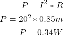
Equation 4: Updated Power equation to find actual power dissipation.
Equation 5 below is the final equation that I use. I calculate the rise time of the MOSFET to be 17.02ns. We can extrapolate this and assume that the fall time will also be 17.02ns. That means that the total time that the MOSFET will be spent switching is 34.04ns. Changing that time into a frequency gives us around 30MHz. Note: I am not using the mathematical definition of rise and fall time (10% -> 90%). I instead am using the physical estimation of the total transition time.
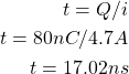
Equation 5: Using the gate charge, we can calculate the rise/fall time.
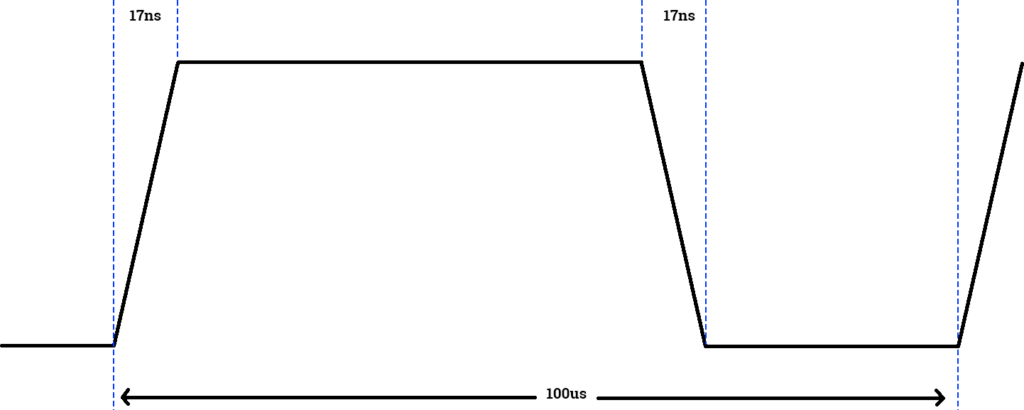
Using the below graphic in figure 7, we can see that with a PWM frequency of 10KHz, it equates to 100us for the total cycle time of the square wave. Since the two 17ns switching transitions take up such a tiny amount of the total time, we can make the assumption that the power losses from them will be negligible. While I don’t have a rule of when this holds true, usually if the switching transition time is less than 0.5% of the total time, I don’t feel worried about using the MOSFET. If however, it gets to where it is taking up a large portion of time, there is a risk of the conduction losses being overwhelmed by the switching, and it overheating.
Testing the Assumption on the Selected MOSFET
In my next blog post, I will post an update on testing this MOSFET in the scenario described. If the selected MOSFET handles the load fine, the next step is to adjust the gate resistor. The larger the gate resistor is, the slower the transition period is. This has the ill effect of increasing the switching losses, but it can drastically reduce the EMI produced on the board. My goal is always to use the largest gate resistor possible, that allows the MOSFET selected to function properly.
Conclusion
Every circuit that requires a MOSFET will have a different set of specs that must be followed. This article gave a pragmatic approach that can be followed for both static and PWM’d loads. I base the calculations and criteria both on simple equations, as well as real-world testing. The next post in this series will build out the scenarios and put the assumptions to the test!
At MicroType Engineering, we specialize in custom electronics design including power electronics and motor control. If you need help designing a circuit or selecting components for your application, contact us to discuss your project.


.webp)