
Designing ESD Protection Circuits
I feel like most (maybe all) circuit designers know that it is important to design with ESD in mind. Most people know the basics (TVS diodes) and try to use them where they can. What becomes a problem, is knowing how much protection you need, and when enough is enough.
This article will focus a lot on general ESD design concepts, as well as putting them into action with LTSpice simulations. Hopefully this will help shed some light on when and where to use ESD protection circuits.
Definitions and Basic Concepts
Electrostatic Discharge (ESD): The release of static electricity when
two objects come into contact.
Device level ESD: An event that occurs to an unmounted
semiconductor in an ESD controlled environment.
System level ESD: An event that occurs to a finished electronic
device/widget.
As a generality, device level ESD is much more likely to cause a failure than system level ESD. The reason why PCB assembly shops are so cautious of ESD is because parts are quite vulnerable before they are mounted to a PCB. Side note: The only example (that I know of!) of an ESD failure that I experienced was from an unmounted MOSFET. The gate must have been zapped before mounting, and it was stuck shorted from source -> drain. This example does not mean that you should be lackadaisical with your ESD protection circuits, instead you should just be more aware when handling un-mounted pars.
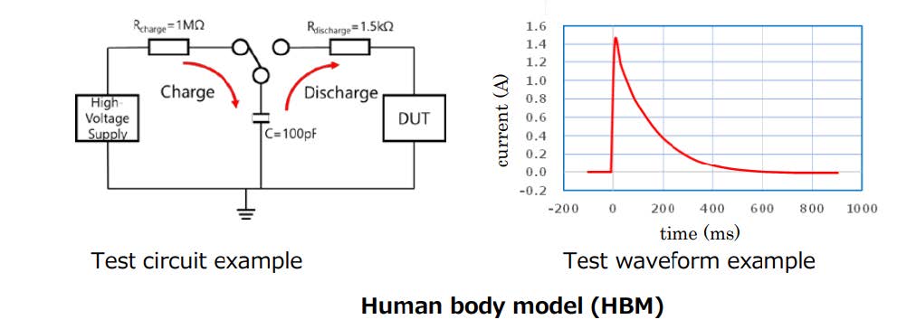
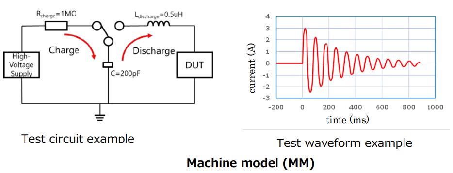
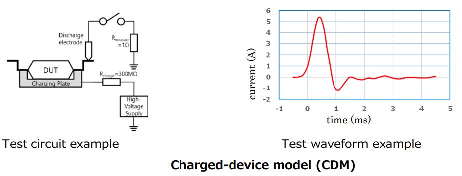
Device Level ESD Tests
System Level ESD Tests
System Level ESD Protection Circuit Goals and Consequences
When a system is subject to an ESD event, whether intentionally during testing, or during the life of the device, there are several outcomes:
- No damage at all – system continues as if nothing happened.
- Soft Failure – No physical damage, but the system has a “lockup” or
“freeze.” May require physical intervention (i.e., power cycle.) - Hard Failure – Physical damage to the system, may or may not show it
immediately (latent defect/failure are the worst).
To elaborate on the latent defect/failure are the worst note: If your device immediately fails due to an ESD or any other type of event, that is bad. If your device takes in damage from that event, but doesn’t fail for a year or two later, that is much worse. You can’t easily troubleshoot the issue . If the ESD event occurs during assembly and a latent defect occurs, testing the device won’t screen out the failure either.
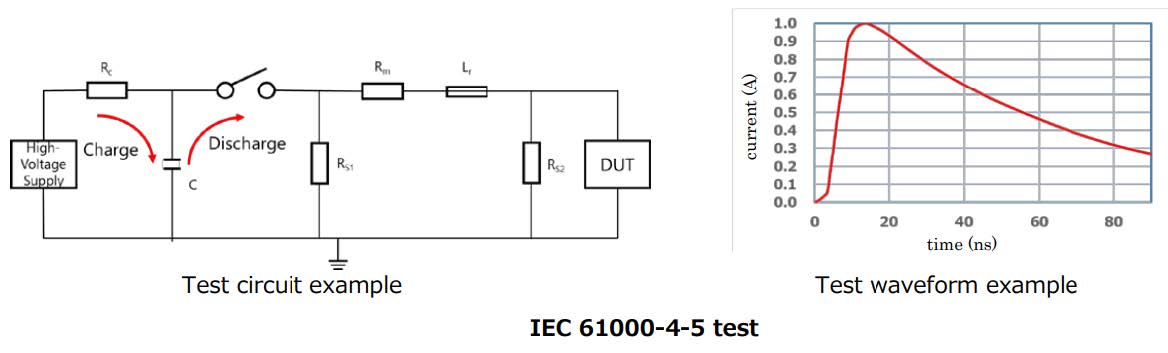
We cover this topic in depth in our article on IEC 61000-4-5 surge protection circuits.
What is the Goal of ESD Protection Circuits?
A common misconception of ESD protection circuits is that you are trying to eliminate the event completely. You then find what looks like a nice 3V3 TVS diode, but see that the clamping voltage is still ~15V. This is well above the absolute maximum of the part you’re trying to protect. So what gives?
All you should strive to do is reduce the event, both in voltage and current. Once it is reduced, the internal ESD protection for the IC can handle what is left.
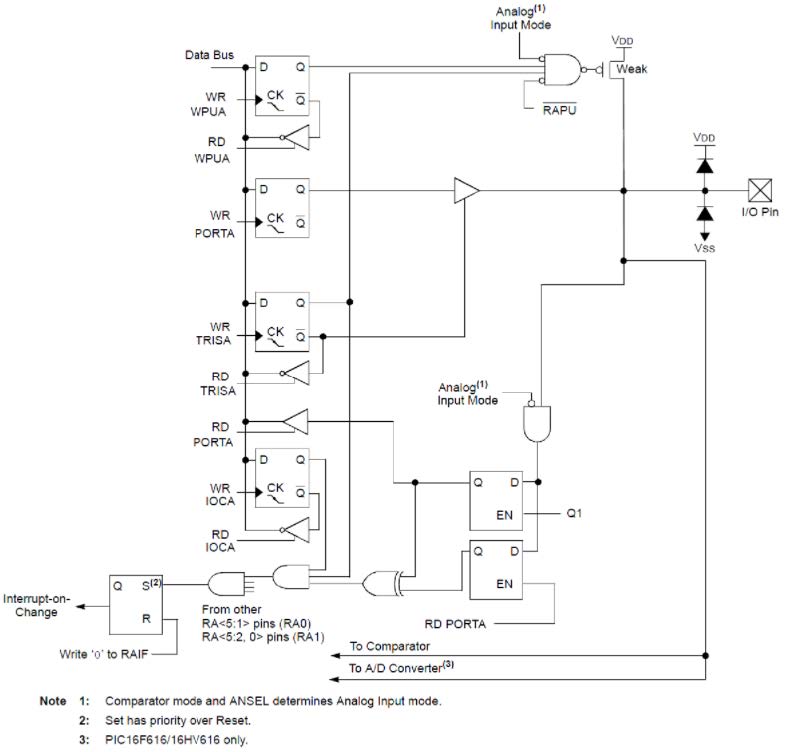
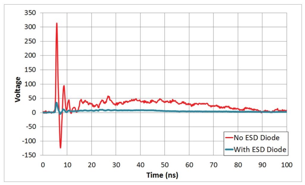
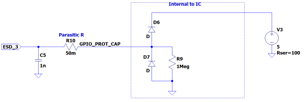
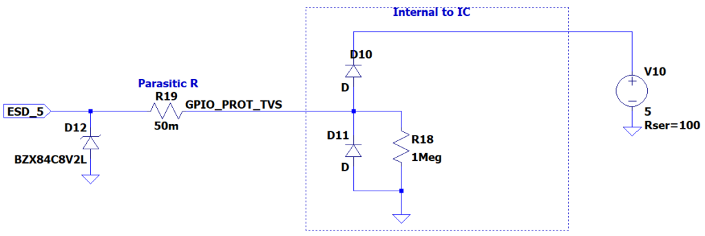
Figure 1 shows the block diagram of a common PIC16 microcontroller. While not all microcontrollers/IC’s will use this exact same ESD protection circuit, they tend to be quite similar. Since the size of these diodes are very small, they can’t handle a lot of current through them without burning up. Figure 2 is a great example of how we can protect these internal diodes. During an ESD event, without an external TVS diode, the IC would see over 300V on its pin. This has a good chance of overloading the internal protection and destroying the device. By adding a single external TVS diode the event reduces both in magnitude and in length of time. This allows the internal diodes to clamp this residual voltage much easier.
Simulation
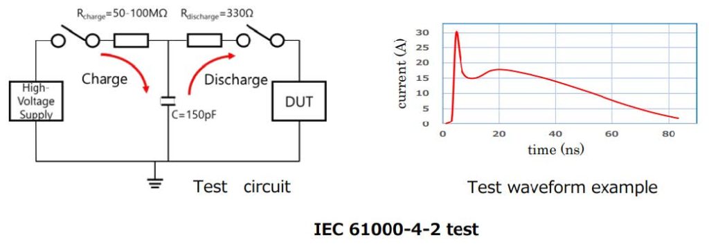
For me to better show how different protection schemes work during an ESD event, I use the following ESD generator in LTSpice.
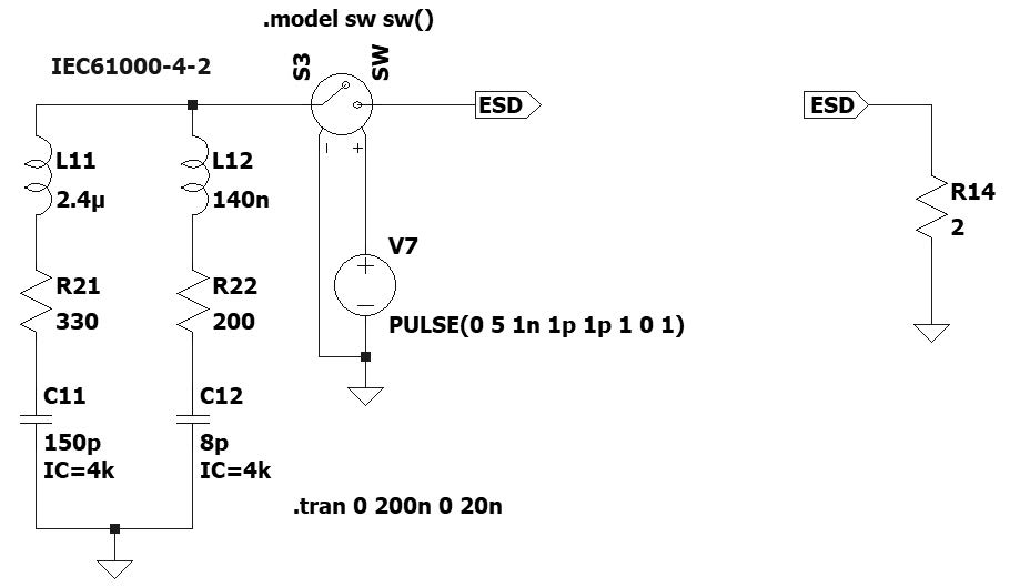
This circuit simulates the test dictated by IEC 61000-4-2. Using a 2R calibration resistor (R14), it produces the following current/time plot:
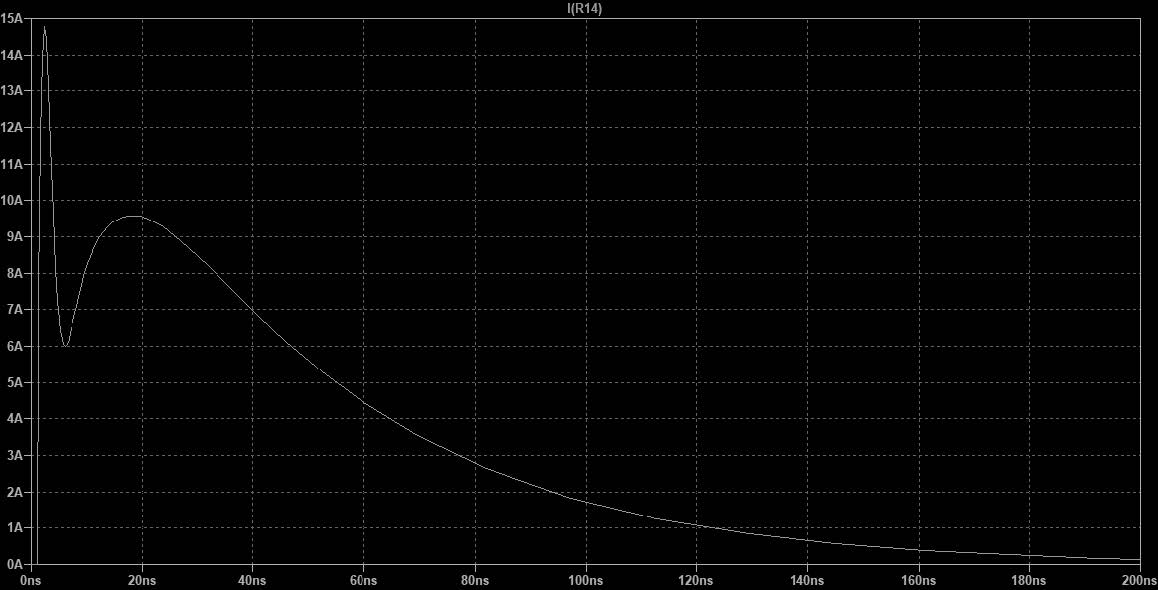
Knowing the baseline, I use this circuit to test a variety of different ESD protection circuits.
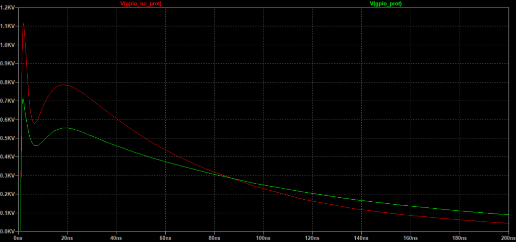
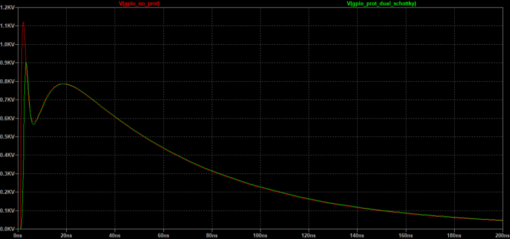
No Protection
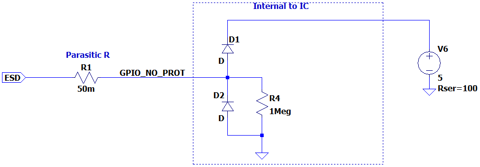
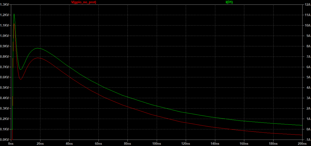
As the plot in figure 6 shows, having no ESD protection exposes the internal protection diodes to an extreme amount of voltage and current. There is a high likelihood that this would cause a failure. Since the current through D1 is directly related to the voltage GPIO, I will only be showing the voltage in future plots to improve clarity.
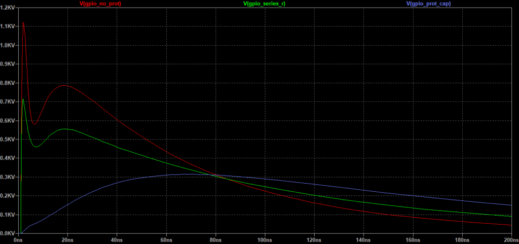
Series Resistors
The first ESD protection circuit I test is simply using a series resistor. For this simulation I use 220R. Series resistors are commonly used to slow the rise time of signals and can greatly improve EMC and SI of a circuit.
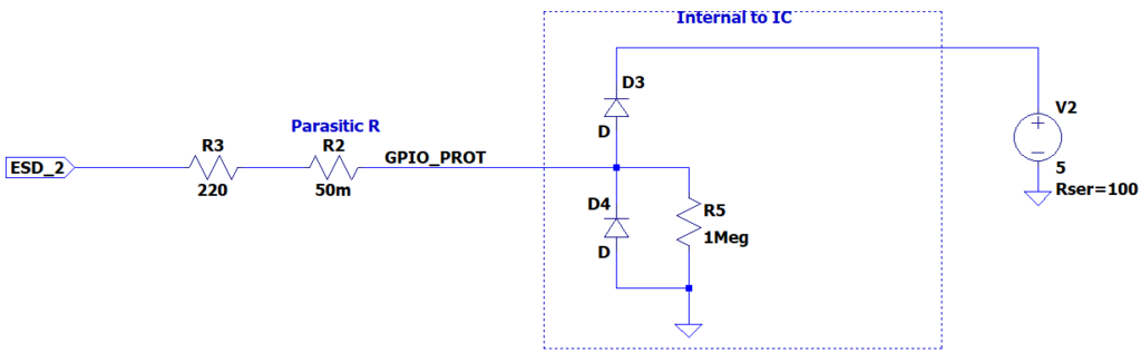
As figure 8 shows, there is nearly a 50% decrease in the maximum GPIO voltage, and a 40% decrease in the current through D10. While this likely would still damage the IC, it does show the impact that a single resistor can make to add ESD protection. If the signal on the IO pins allows for it, a larger resistor provides additional protection.
Capacitors
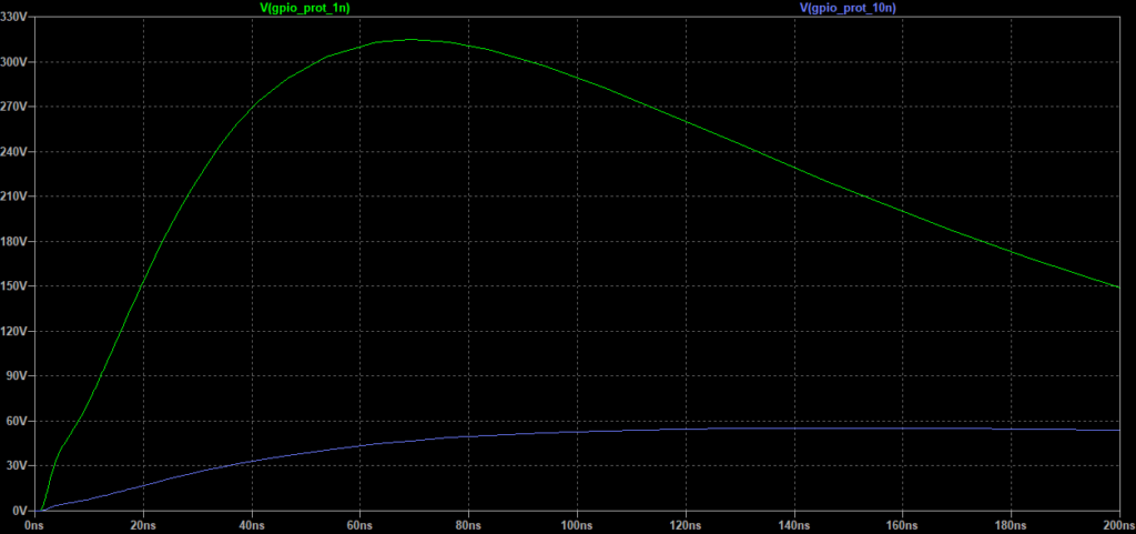
Another simple ESD protection circuit is to simply add a capacitor from the pin to ground. Similar to the series resistor, the size of the capacitor is dependant on the intended use of the line.
As shown in the plot in figure 10, a single small 1nF capacitor makes a drastic difference to the plot. The peak voltage is less than 330V, and it limits the current to around 3A. Once potential issue with this ESD protection circuit is that the event is now much longer. This has the possibility of overheating the internal protection diode, as well as having a greater chance of corrupting any data on this line.
The same is true as with the series resistor, the larger the capacitor, the more protection it provides. One exception is that a large ceramic with low ESR can cause ringing. So normally you use a series resistor in conjunction with a capacitor, or at least damp the capacitor with a resistor in series with it. Also, to state the obvious, you can’t use this approach with any communication or high-speed signals, as the capacitance will load the bus too much. For more on how ceramic capacitor behavior changes under DC voltage, see our article on the DC bias effect.
TVS Diodes
Finally we come to TVS diodes, one of the most commonly used methods for an ESD protection circuit. They essentially act identical to a zener diode, but conduct faster and have a higher surge rating. (They also sometimes don’t have a specified continuous current/power rating). There are a few important definitions/specifications:
- Reverse Working Maximum Voltage (VRWM): The maximum reverse voltage that should be applied in normal operating conditions.
- Breakdown Voltage (VBR): The voltage where the diode just starts to conduct.
- Clamping Voltage (VCLAMP): The maximum voltage that the system will experience during a surge.
- Dynamic resistance (RDYN): The estimated resistance of the diode when fully conducting.
Something that is commonly misunderstood is the use of bidirectional vs unidirectional diodes. The only time to use a bidirectional TVS diode, is to protect a differential style signal that goes above/below 0V. Example: RS485. AND8424/D from OnSemi is a great appnote that explains this in more detail.
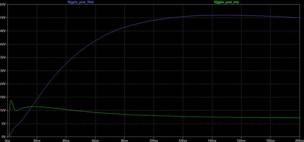
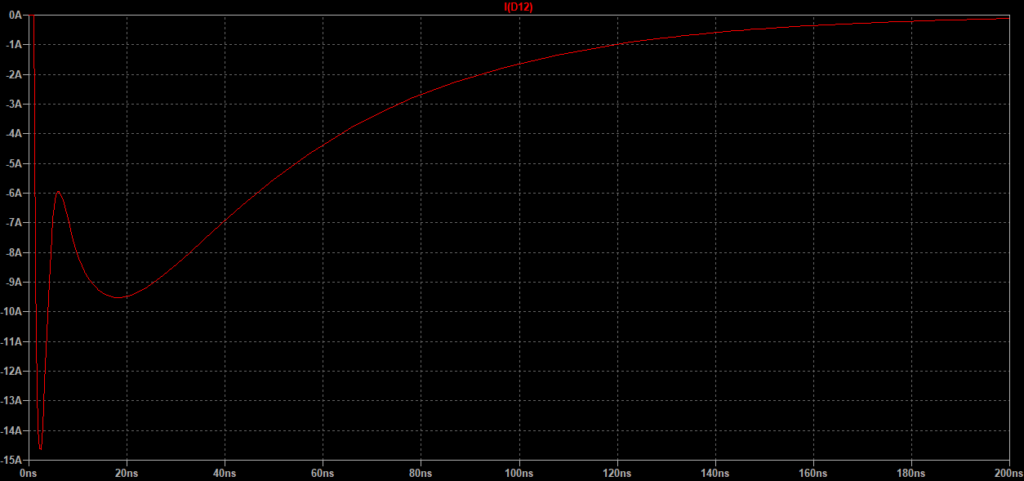
As Figure 13 shows, this is by far the most significant protection of any method thus far. The maximum voltage is now around 16V and the current through D10 is barely 100mA. The internal protection diodes can certainly handle an event like this without any risk of damage. Something important to understand is the amount of stress that the external TVS diode, D12, is subjected to. This is shown in figure 14 below.
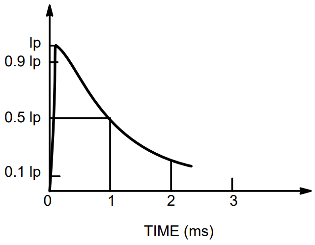
TVS’ Current rating
When using a TVS diode (instead of a zener diode), the datasheet will provide a specification of “Current – Peak Pulse (10/1000µs)”. This is the maximum rated current the TVS diode can handle over a specified amount of time and waveform. This waveform (sourced from OnSemi AND8308/D) is in Figure 15. For a more detailed look at TVS diode selection and placement, see our article on the usage and function of TVS diodes in circuit protection.
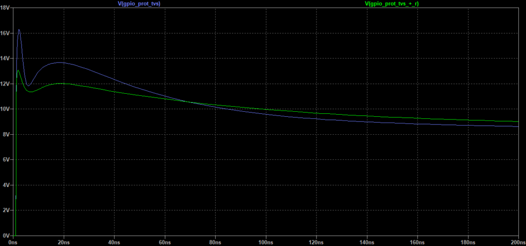
A simple way to reduce this current and protect the TVS diode is to use a series resistor on the connector side of the TVS. This circuit and plot are shown in Figures 16 and 17, respectively.
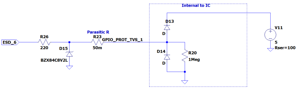
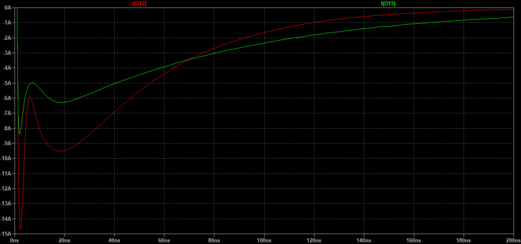
Once again, when the peak current/voltage of an event reduces, the length of the event increases. As you would expect, this resistor also has an impact on the peak voltage on the GPIO pin. This plot is in Figure 18 below.
Dual Schottky Diodes
Another interesting ESD protection circuit that I use from time to time, is dual schottky diodes. You bias one to ground and the other to the input voltage rail. What makes this different than the TVS approach is that during a positive voltage spike, the power is dumps to the positive rail, not ground. This means that for this approach to be effective, there must be a low impedance power distribution network in place.
Consider the circuit in Figure 19 below.
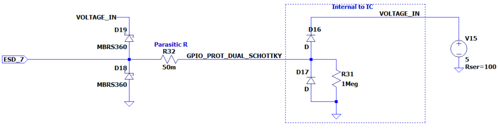
Notice that V15 (the power supply) still has the rather large series resistance of 100R. This means that on a positive ESD event, the surge essentially travels through D19, then a 100R resistor, before completing the circuit through ground. As Figure 20 shows, this is not a very effective protection scheme.
Another issue to watch out for with this scheme is the reverse voltage rating on the Schottky’s. It is easy to exceed it and damage the diode.
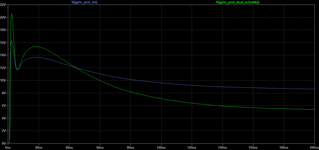
Considering that most power supplies have well under a 1R impedance, this scheme can be quite effective. It is crucial to understand you power distribution network if you use this approach.
What ESD Protection Circuit Do I Normally Use?
I know that this was a very picture heavy article covering a lot of different options. I will wrap it up with a discussion on what I use where, and why. Most signals/protection can be broken up into three categories:
High-Speed (USB/Ethernet/HDMI/Etc.)
Signals that fall into this category are normally pretty easy to design protection for. This is due to there being quite detailed specifications for the maximum bus capacitance that each signal can have before degradation occurs.
I typically will use a TVS diode specifically designed for the signal type. I then will see if series resistors are acceptable, and will use the largest value possible.
Slow Interface, General Protection
These are your general purpose pins that leave the board. Maybe it’s for an LED or a switch. Or it could be for a touchpad. The key here is that it won’t be subjected to a brutal environment, and/or it is a inexpensive product.
For these I will typically use a TVS + a large series resistor. Depending on the application, I may use the dual Schottky approach instead. The reason is that you can also provide over current and short circuit protection.
(If you would like a full article on over current protection schemes, please drop a comment!)
Slow Interface, High Protection
This is quite similar to the above, except this is for industrial applications, or situations where a failure is not acceptable. For this, I will add an additional capacitor to the signal, reducing the slew rate significantly.
ESD Protection Circuits Conclusion
While there are many ways in which to protect a GPIO pin from ESD damage, they don’t all provide the same level of protection. Simply adding a series resistor and a capacitor can provide significant protection. A properly selected TVS diode can also work equally as well. It is crucial to understand the environment that the board will be in, as well as the signal type. Using a simulation tool like LTSpice is an excellent way to validate the protection scheme.
MicroType Engineering specializes in custom electronics design with a focus on robust, reliable circuits. Whether you need ESD protection designed into a new product or firmware support for an existing design, reach out to learn how MTE can kickstart your new design today!


.webp)