Rise Time and Series Resistors
Introduction
When designing electronics, people tend to think that the raw data rate of a signal rules all. The thought is, the faster the data rate, the harder it is to have good Signal Integrity. A higher data rate will have worse Electromagnetic emissions. While this certainly can be true, it is also a gross oversimplification.
Often, one of the most significant factors of whether or not a signal will radiate, is the rise time of the signal. It is true that to have a high-speed interface, you need a fast rise time. Unfortunately, there are also many low data rate digital ICs that still have incredibly fast rise times.
In this article, I show the importance of rise time on EM radiation. By using a series resistor near the sending IC, it forms an RC filter with the capacitance on the receiving component/IC. By varying the value of the resistor you can lower the rise time for the needed data rate.
How to Test?
To test varying rise times, I chose a LTC6905. It is a variable frequency oscillator from Analog Devices. The specific part that I used was the LTC6905IS5-96, which has a fixed master clock of 96MHz. By adjusting the DIV pin (LOW/FLOATING/HIGH), the master clock divides out by 4/2/1 respectively. This allows us to have an output of 24MHz, 48MHz, and 96MHz.
The main reason I chose this part is the specified rise time. According to the datasheet, it has a rise time of 0.5ns with a 5pF load capacitor. It also can drive a surprisingly large load (4mA) for an oscillator. To be able to validate the exact rise time, you would need a several GHz bandwidth oscilloscope, which I do not have. Since we’ll be comparing the part against itself, the exact rise time isn’t important, only that it is fast!
Test Board
Schematic
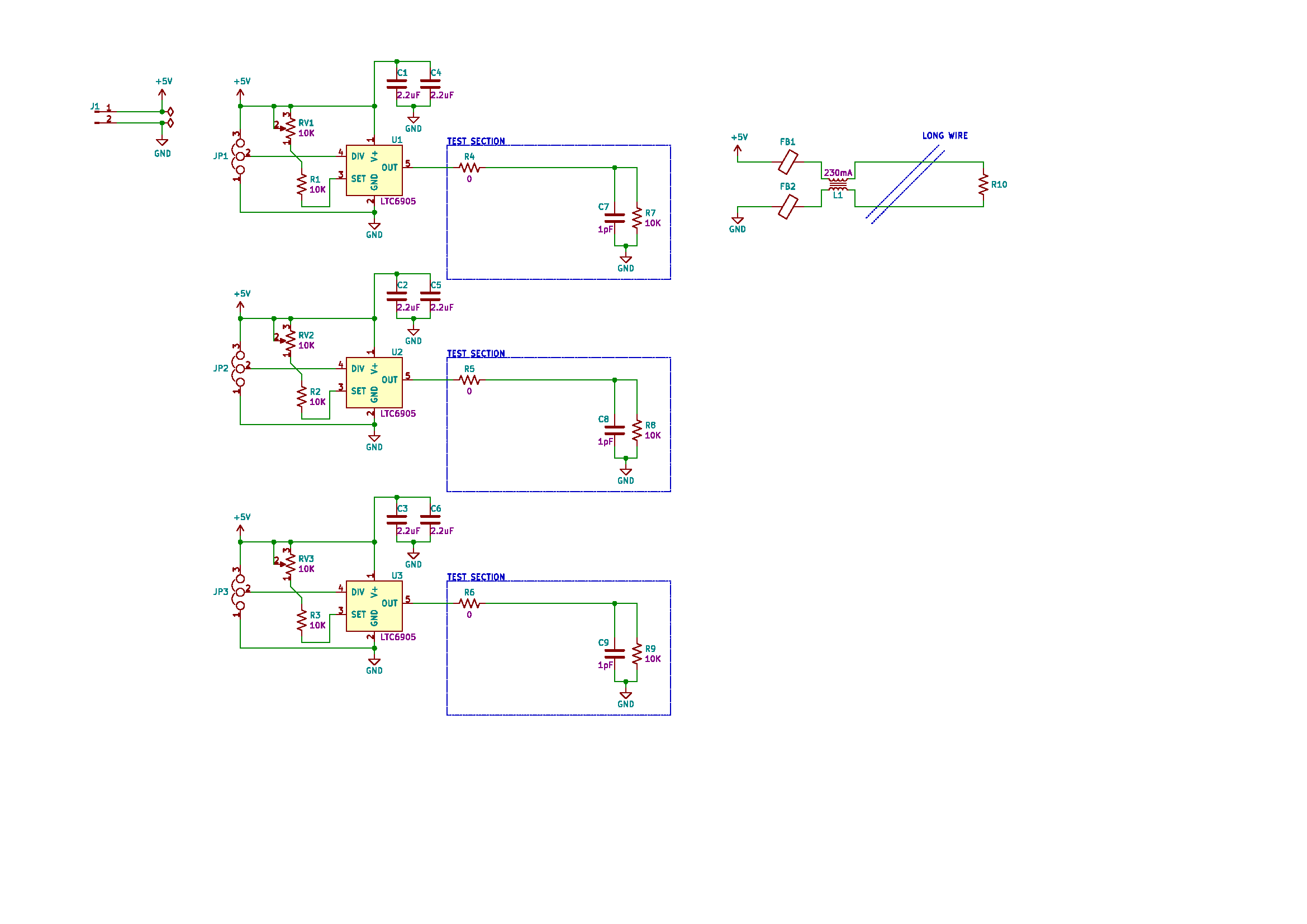
Figure 1: Schematic of the test board. 3x identical blocks based on the LTC6905 oscillator
The schematic above is quite simple. It consists of three identical blocks based on the LTC6905. Each block has 2x 2.2uF 0402 decoupling capacitors, with an adjustable jumper on the DIV pin to set the clock divider. The SET pin has a voltage divider which the specific LTC6905 I chose doesn’t use, so I did not populate it.
The oscillator output goes through a series resistor and then drives a 10KΩ resistor in parallel with a 1pF capacitor. To test any common mode currents that the driver generates, there is a wire that takes 5V/GND and leaves the board.
PCB
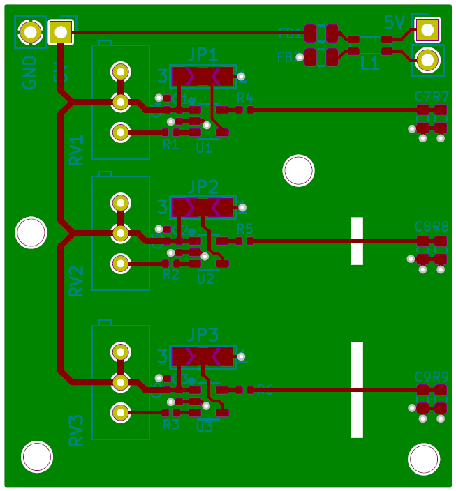
Figure 2: The test board PCB. Notice the return path discontinuities where the return current must go around.
The above PCB shows the three blocks laid out as identical to one another as possible. The only difference between them is an increasing in size return path discontinuity in the bottom ground pour. There is not a top ground pour, forcing all return currents to go on the bottom layer, around the discontinuity.
For all tests in this post, I will be using the furthest South block. Any radiated emissions will be amplified because of the larger loop area in the return. The top two blocks were disconnected from power to ensure they wouldn’t impact the testing.
Testing Methods
Near-Field Probe
The most effective method to see the emissions from a single trace is to use near-field probes. They pick up the electromagnetic radiation from a trace in the near-field. There are both magnetic (H-Field) and electric (E-Field) probes. It is critical to understand that any measurement taken from a near-field probe is qualitative in nature. They can not be directly correlated to any EM compliance standard.
I’m not going to get into the “nitty gritty” of why that is in this post, but a quick summary: In the near-field, the EM field is dictated primarily by the circuit impedance, with either the E-Field or H-Field being dominate independently. While in the far-field they act as “real” EM waves, with a wave impedance of 377Ω. There is a great article on the topic here.
For my tests, I mark a single location above the return path discontinuity where I place the probe for each test. I use an E-Field probe as they are smaller, making it easier to pinpoint a specific location.
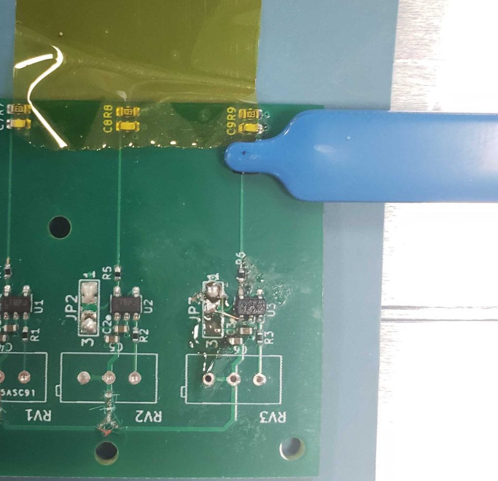
Figure 3: The E-Field probe is place directly above the return plane discontinuity. (Ignore the horrible flux and rework, this was taken after all tests were conducted!)
Common Mode Current Clamp
A really useful pre-compliance tool is an RF current clamp. In fact, Henry Ott stated in his famous EMC book that it is the single most importance pre-compliance test that you can do. The reason why is pretty simple:
- First, it is a really easy test to do. You don’t need any sort of elaborate test setup, and it’s quick to complete.
- Second, to have radiated emissions, you need both an energy source and an antenna. Cables that leave a PCB will be several times longer than any single trace on the board. This gives them a much greater chance than traces to radiate.
These probes measure the amount of common mode current flowing in a cable. To be clear, all common mode current is unintentional, as it’s not the driving signal. There are several correlation equations to convert the power of the RF energy to a current. You can see what the limits are at any given frequency.
Since I will only be comparing results to other results, I will just use the raw RF data from the clamp.
Results
Importance of Resistor and Probe Location!
When I first was conducting tests, I started with a 0Ω series resistor. I placed the E-Field probe in between the IC and the resistor, as it was an easy place to index the probe. I checked all along the trace to confirm that the location was accurate, which it was.
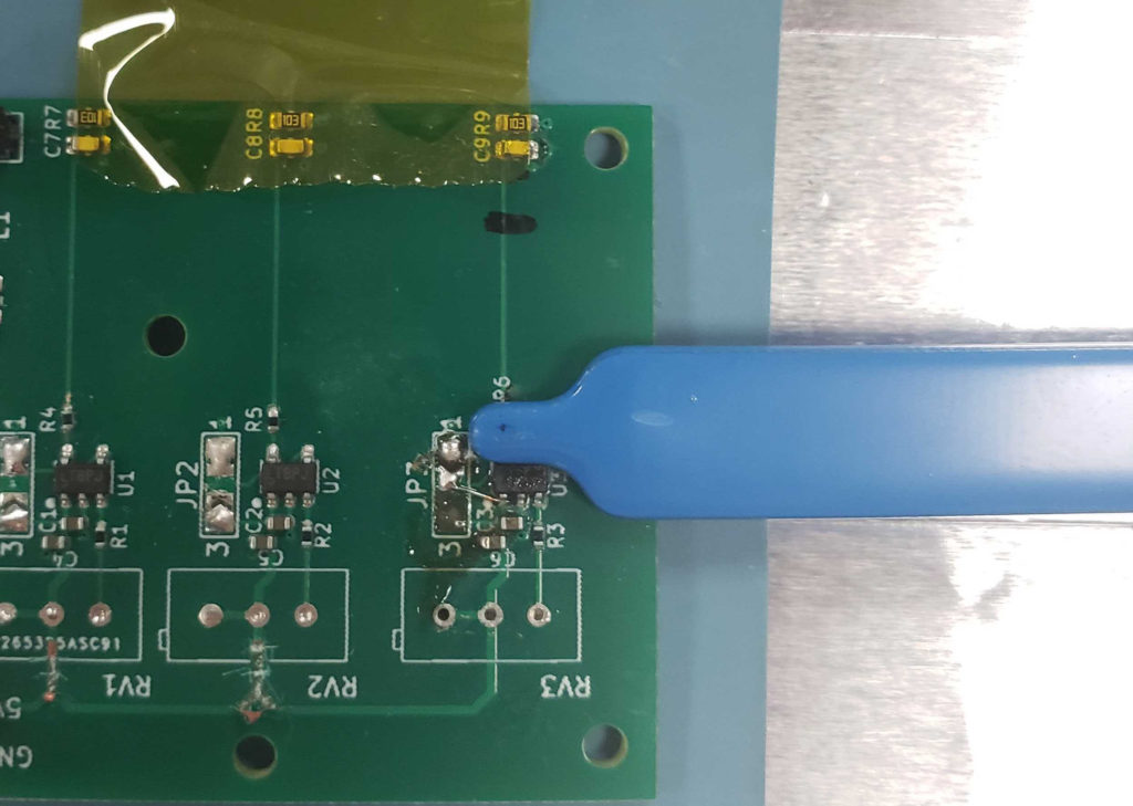
Figure 4: The E-Field probe is place between the driving IC and resistor. (Ignore the horrible flux and rework, this was taken after all tests were conducted!)
Then, I recorded test data at 96MHz and 48MHz, using a 0Ω, 220Ω, and 10KΩ resistor. When analyzing the data, it was confusing to me, as there was essentially no difference between the different resistor values.
I then realized that since I only checked along the entire trace at 0Ω, I didn’t actually confirm that this location was correct. The series resistor does not effect the rise time of a signal from the IC to the resistor. This is something that is really important and I will come back to later in this post.
E-Field Probe: 96MHz
Now that I knew exactly where to probe the trace (directly over the return path discontinuity shown in figure 3), I redid all tests. I started with the LTC6905’s master clock at 96MHz
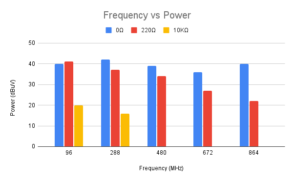
Figure 5: Frequency vs Power with the IC clocked at 96MHz. Above 288MHz there were no peaks with the 10KΩ resistor.
The above graph shows the power of the radiated emissions at the fundamental frequency, 3rd, 5th, 7th, and 9th harmonics (96, 288, 480, 672, and 864MHz respectively).
E-Field Probe: 24MHz
Then I conducted the same tests with the IC clocked at 24MHz
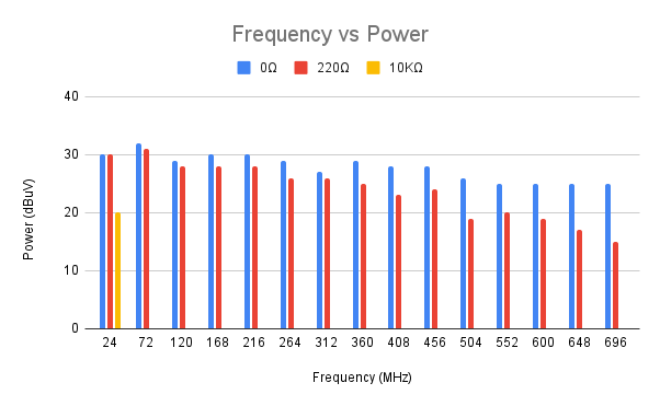
Figure 6: Frequency vs Power with the IC clocked at 24MHz. Above 24MHz there were no peaks with the 10KΩ resistor.
The above graph shows the power of the radiated emissions at the odd harmonics out to the 29th.
RF Current Clamp: 96MHz
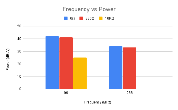
Figure 7: Frequency vs Power with the IC clocked at 24MHz. Above 96MHz there were no peaks with the 10KΩ resistor. Above 288MHz there were no peaks with any resistor value.
The final testing was with the RF current clamp. I only am showing the results when clocked at 96MHz, as the trend is identical when at 24MHz.
Discussion
Fourier
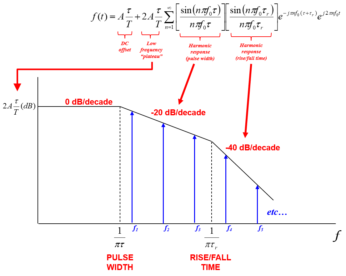
The above image shows the Fourier transform of a trapezoidal square wave. Keep in mind that all real world square waves are trapezoidal! There are constant terms, a waveform response term, and a response term based on the rise/fall time.
What is important to see is that once the signal hits the point where ƒ=1/(π*τr) the power decreases at a rate of -40dB/decade. Before this point it decreases at -20dB/decade. By increasing the rise time, we effectively shift this point to the left, decreasing the bandwidth of the emission.
Real World Impact
While the Fourier transform is nice to cover in theory, what does it all practically mean?
It means, that while the fundamental frequency does have an impact on EMI (Especially when considering detection types other than peak, like quasi peak); the rise time of a signal is much more important when trying to limit EM radiation.
Whenever possible, you should use series resistors to slow down the rise time of signals. Of course, you can’t always do that, but often times, digital ICs will have a much faster rise time than is required for what it is driving. If you’re using a shift register or an i2c expander to drive indicator LEDs, you don’t need a 20ns rise time!
As I mentioned earlier, when I initially tested with the probe between the IC and the series resistor, there was basically no impact of changing the resistor value. This shows, as you would expect, that it is crucial to have the distance from the driving IC and the series resistor be a short as possible. Since that trace will radiate as if there is no resistor, you want to reduce the size of its antenna as much as possible.
Conclusion
The goal of this article was to highlight the importance of signal rise time in EMC. By simply including a footprint for a series resistor on every digital signal trace, you have the ability to slow down the rise time. This will decrease the bandwidth of any radiated emissions from these signals. While you can sometimes calculate the exact resistor value, often it is a matter of trying a few values, ensuring there is no data loss.
As always, it is critical to make EM compliance a core part of the initial circuit design process. Here at MicroType Engineering, we specialize in high quality PCB design and pre-compliance testing. Please reach out to learn more about our process.
Recent Comments