
Why Does it Matter?
When discussing conducted emissions, often you think of the AC line going back into the power grid. It is easy to ignore the DC section that the AC/DC regulator is powering. While it is true that most testing standards don’t test the DC portion during emissions testing, that doesn’t mean it is not important. Plus, certain environments (mainly automotive) do test the DC lines for conducted emissions. If the DC portion of a circuit is emitting a large amount of conducted emissions back onto the DC line, you essentially are dependent on the AC/DC converter to properly filter this.
Unless you specify (or build) the exact AC/DC converter, this assumption often is not a safe one. Instead, you should always ensure that all input wiring, regardless if it is mains AC or DC is properly filtered for conducted emissions. Then, unless the AC/DC converter is spewing its own emission onto the mains line, you can be certain that your side is not.
Why a Buck Convertor?
Buck converters are typically the main reason that a device fails conducted emissions. Due to the nature of the switching loop, there are large current transients (dI/dt) on the input side. The output side of the regulator is well filtered due to the inherent LC filter. A boost regulator is the exact opposite (transients on the output side). Since most regulators have a switching speed of less than a few MHz, they are in the prime range of conducted emissions testing.
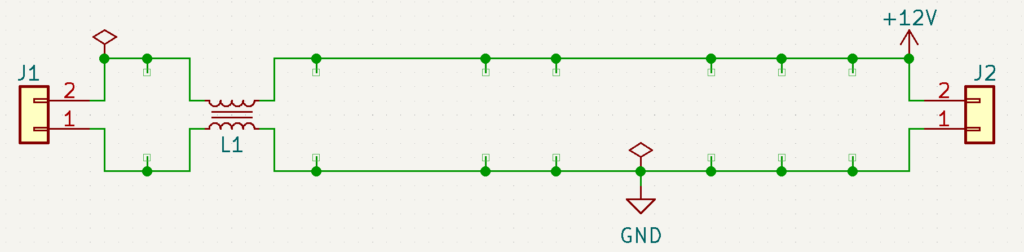
The Test Boards
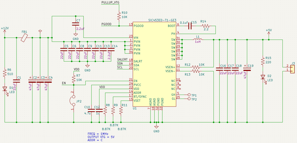
Buck Converter
The primary board that I am using for testing is the same board that I featured on the first EMC For Everyone Series and the High Power Buck Convertor livestream. There is a large amount of low ESR ceramics, electrolytic’s, and a small ferrite on the board. However, it likely would still fail conducted emissions testing. Figure 1 shows the schematic of this board. It can output up to 15A at 5V.
Filter Board
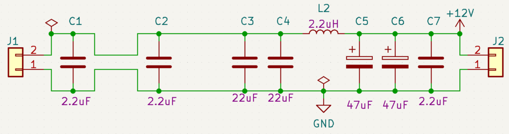
To avoid building a new (or multiple!) buck converter PCB’s, I instead built a filter board to go in-between the buck and the input power supply. Figure 2 shows this board. It can filter common mode noise using the common mode choke, and differential noise with the Ferrite’s and PI filter.
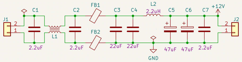
Throughout testing, I will remove and add sections of this board to selectively test certain elements.
Testing
I will first go through all tests that I did. Then I will dive into the discussion of the results and what they actually mean! The blue limit line in all the spectrum analyzer traces is the conducted emissions standard EN 55022/32 Class B. I will be using the limits for Quasi-peak, while my results will be measuring peak. This makes my testing more stringent, which for pre-compliance testing is always the goal. The board uses an input of 12V and an output of 5V at 8A.
The buck convertor board for all tests will have all elements populated except the ferrite bead. The bead will be shorted across with a small copper wire.
All Bypassed
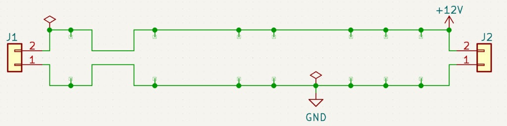
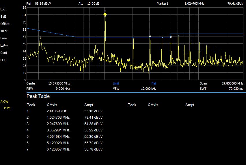
The first test was essentially testing the buck convertor board alone. All series elements were shorted across with a small copper wire. All capacitors were removed.
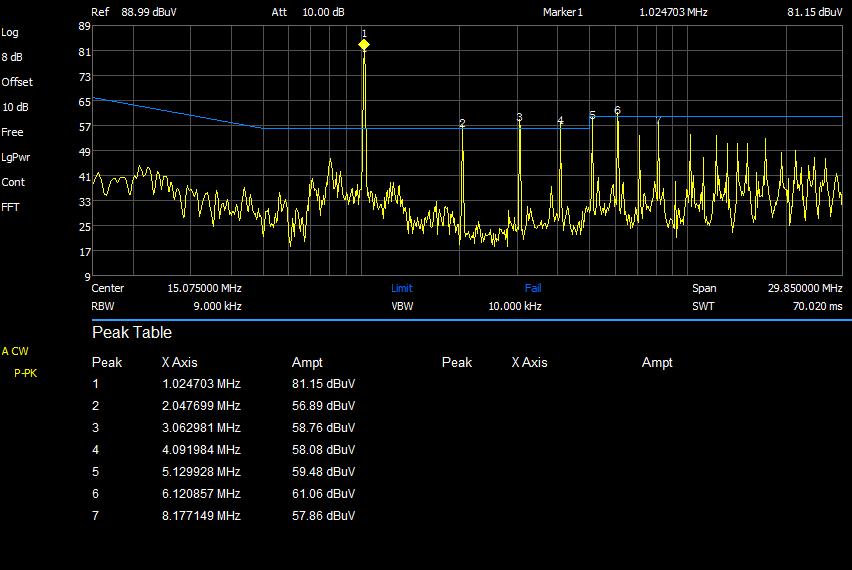
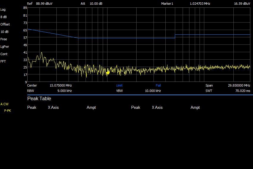
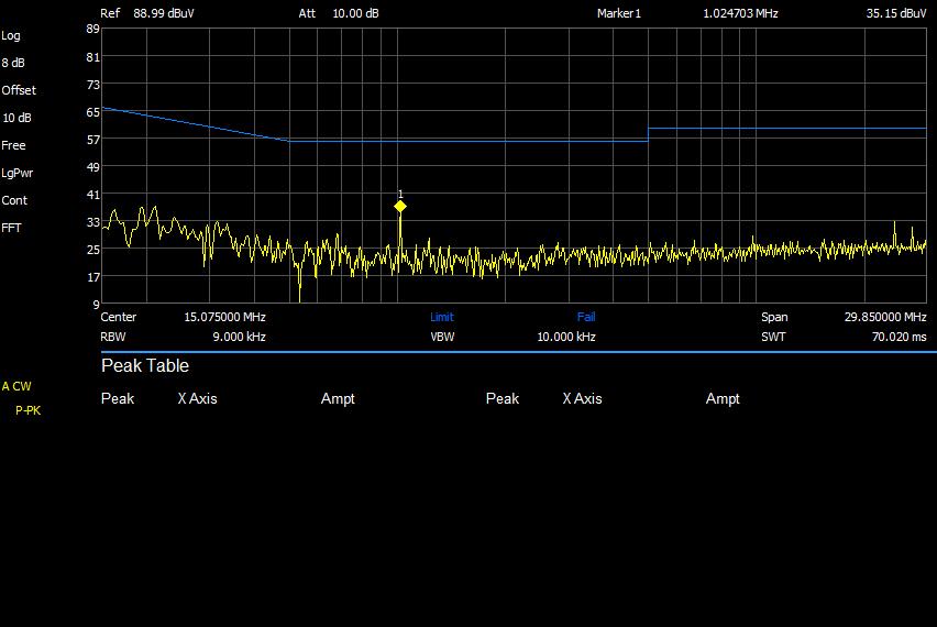
The results of this test are shown below in figure 4. The fundamental frequency of 1MHz has a amplitude of 81dBuV and is quite clearly over the limit. The next 5 or so harmonics are right near the limit.
Testing The Common Mode Choke
The second test was much like the prior one. This time I populate the common mode choke, shown as L1 on figure 5.
The results are shown below in figure 6. The amplitude of all harmonics including the fundamental decreased by a few dBuV. The fundamental is still drastically exceeding the limit, while the others are right at the edge. Interestingly, there is now a peak at around 210kHz. It is at 55dBuV, around 8dBuV below the limit.
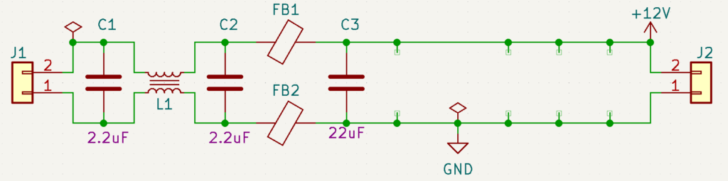
Adding Some Differential Filtering
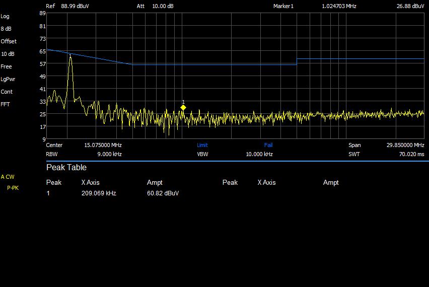
The third test was to add both ferrites, and some ceramic capacitors as shown below in figure 7.
The results of this test are below in figure 9. It is pretty clear the massive improvement that was made. Interestingly, the peak at 210kHz actually worsened by around 5dBuV. It is now right at the limit line, nearly touching it.
Confirming the Source of the Peak
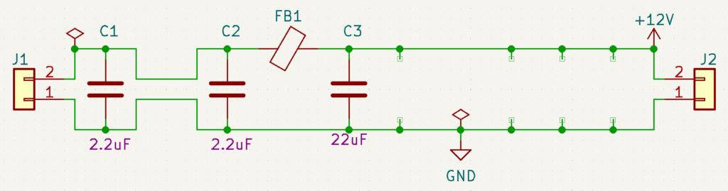
To be absolutely certain that the cause of the 210kHz peak was the choke, I removed it. The schematic for this test is below in figure 9.
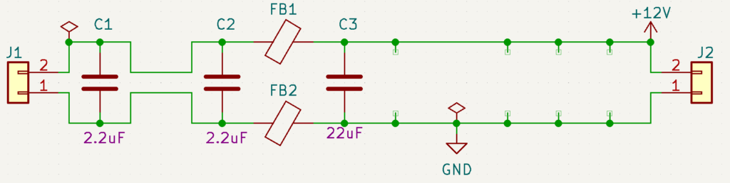
Figure 10 below shows the results of this test. It completely removes the peak at 210kHz, and the trace is essentially perfect. There are no peaks that come anywhere close to the limit.
But What About the Second Ferrite?
The reason why I have two ferrites on the filter board I’ll cover in the discussion. But, to ensure that the second one isn’t the only reason the board did so well, I will remove it. The schematic of this test is figure 11.
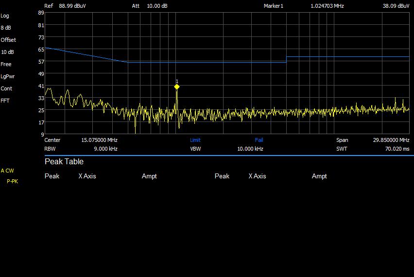
The figure 12 above shows the results of this test. There is now a peak at the fundamental, but it is below my peak table limit. It appears to be right around 40dBuV, which is nearly 20dBuV below the limit line.
The Pi Filter
The final test was to populate the PI filter. This involves several capacitors and the inductor, L1. While some of the capacitors were populated on prior tests, they will have negligible impact for this one.
The results of this test are below in figure 14. The results are essentially the same as when using a single ferrite. The fundamental peak may be a couple dBuV lower, but not much.
Discussion
Filter Board Bypassed
The first test that I performed was simply bypassing all of the filtering on the filter board. This was to show how the buck convertor board performed without any additional filtering. Much like in the first video, the board showed a horrible peak at the fundamental frequency, with harmonics that were close to the limit. As I’ve mentioned in the past, a safe rule of thumb to have is that a buck convertor will fail EM compliance testing unless there is a series filter element. No matter the amount of low ESR capacitors you use, you typically still need some sort of series filter.
Common Mode Choke
The next test simply added in a large common mode choke. I knew that this wouldn’t help things much, since the normal failure mode is differential noise in a buck convertor. As long as you have a good layout with small loops, common mode noise isn’t normally a concern in a board like this. What did surprise me was the nasty peak at 210KHz. That was likely just a result of the large coils causing an resonance point.
This shows why it is so critical to make pre-compliance testing an integral part of any new product development. You can't just skim a datasheet and learn that it has a random resonance peak that could cause it to fail an emissions test.
Importance of Ferrite Selection
Once I added the two ferrites the emission was essentially eliminated. Since the original buck convertor board had a small ferrite in its design, why didn’t that help? Well the answer is actually quite simple:
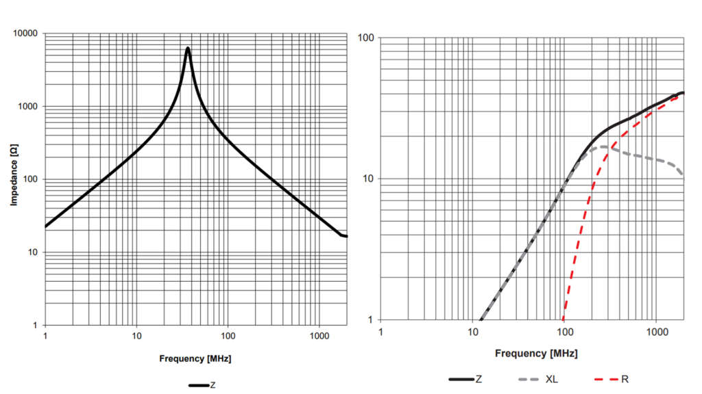
Figure 15 shows the differences between the two beads using their ZRX charts. As a refresher, the ZRX chart shows the impedance of the bead at different frequencies. (Technically the left chart just shows the overall impedance)
Since we are concerned with frequencies below 30MHz, it’s clear why the ferrite on the left out-performed the original bead. The original bead only started filtering at 12MHz. It also has an impedance of several orders of magnitude less.
Why then, did I not just choose the left bead at the start? Simple, it is significantly larger, and I wanted the board to be compact. This goes to show why understanding design choices and compromises is so crucial to a successful PCB or product design.
Multiple Ferrites
The reason I included two ferrites in the filter board was simply so I had the ability to test it in a common mode configuration. With a ferrite on the positive and return side of the input, they can filter both differential and common mode noise. Since we saw that there was no common mode noise, only one ferrite was needed. Note: the second ferrite helped filter differential noise more effective, simply because it was in series with the first. This effectively doubled the impedance to differential noise.
Pi Filter
The final test was to short out the ferrites, and add the Pi filter in. This performed nearly identical to the single ferrite test. There was only one peak at the fundamental of 37dBuV. Since both approaches worked quite well, which option should you choose? Well, I don’t have an amazing answer to that!
Me personally, I tend to default to a Pi filter. I find them easier to design with, and they don’t have a DC bias effect like a ferrite. When the DC current through a bead increases, the effectiveness of a ferrite bead decreases. Sometimes up to 80% or more. With an inductor, as long as the current is below the saturation current, it will not noticeably impact the filtering characteristics.
Also, the ferrite that I used on the filter board is honestly an anomaly. Most ferrites are more in line with the smaller bead I originally used. They don’t have much impedance until 10s to 100s of MHz’s. This makes them useful for higher order harmonics and digital switching filtering, not so much for buck convertors.
Conclusion
A rule of thumb I follow and tell others is that any time an input power line on a PCB goes into a buck converter, it should have some type of series element. In this article I showed while even though low-ESR capacitors are necessary, a proper series filter is needed. It is sometimes possible to select a ferrite bead that can filter at these low frequencies. A sometimes easier option however, is to instead use a Pi filter tuned for the frequencies of interest. (Stay tuned for a full article and video on how I do that!)
Common mode chokes can certainly be helpful sometimes. However, the choke I used for this test shows not always are they needed or a even a good option. This also highlighted how imperative a pre-compliance test lab is for product design. Here at MicroType Engineering, we specialize in high quality PCB design and pre-compliance testing. Reach out if you need help with EMC or power supply design.


.webp)