Understanding how to properly troubleshoot circuits is an important skill to possess as an electronics designer. No matter how well versed in design and layout you are, many days will be spent on time-consuming circuit troubleshooting. It is crucial to have a solid understanding of circuit design basics, and also have the equipment available. This design required an oscilloscope, a soldering iron, and a few resistors and capacitors to troubleshoot.
This article discusses a high powered LED board. We designed it based on detailed specs from our client. Power comes from a single 24VDC supply – for testing, we used a 30A Extech adjustable power supply (PSU). There is a total of 100 LEDs, with 11 different types of LEDs. The distribution of LED strand length and forward voltages is very inconsistent, leading to a challenging design from the start. Much of the PCB layout techniques is from the information I shared in the High Power PCB Design Tips & Tricks article. I will not be discussing the PC Board layout in this post.
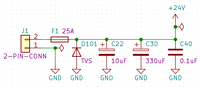
Image 1: The main input supply of 24VDC. Power passes through the fuse, capacitors filter it, and a TVS diode protects from transients.
Design Background
The most challenging part of this design was determining how best to drive the LEDs. We needed to have full brightness control, as well as minimizing the heat generated. The first choice was to use constant current LED specific drivers, both linearly driven, and also drivers with internal switching regulators. We eliminated the linear drivers almost immediately. The LED strands were driven at around 1 amp each, and some strands would only have four LEDs. With a forward voltage of 3V, for example, this requires the driver to dissipate (24V – 3V * 4) * 1A = 12 watts. 12 watts is much more power than most drivers can safely dissipate.
The next option – and the one that I had initially planned on using – was to use a separate switching driver for every strand. The advantage of this approach is that every strand can run very efficiently since most modern switching regulators have well over 80% efficiency. The drawback with this was that since we are using a 24VDC supply, we weren’t able to group all 11 LED models on just 11 strands – we didn’t have enough voltage headroom. We required 18 different strands. The PCB was rather large, but the idea of having 18 switching regulators switching high power loads wasn’t something that I felt comfortable doing, unless there wasn’t any other option.
Combination Linear and Switching Supplies
What we decided to use was a sort of “hybrid” approach. We designed several of the strands, so they had a few volt headroom on the 24V supply. For example, one type of LED had a forward voltage of 2.8V. Using 8 of them on a single strand, we only had to drop 24V – (8 * 2.8V) = 1.6V. When driven at 1A, this is only 1.6W to dissipate – easily done with one or two high power resistors.
In total, there were nine strands of LEDs that we could drive this way – nearly half of the required strands! Image 2 shows and example of two of these strands.
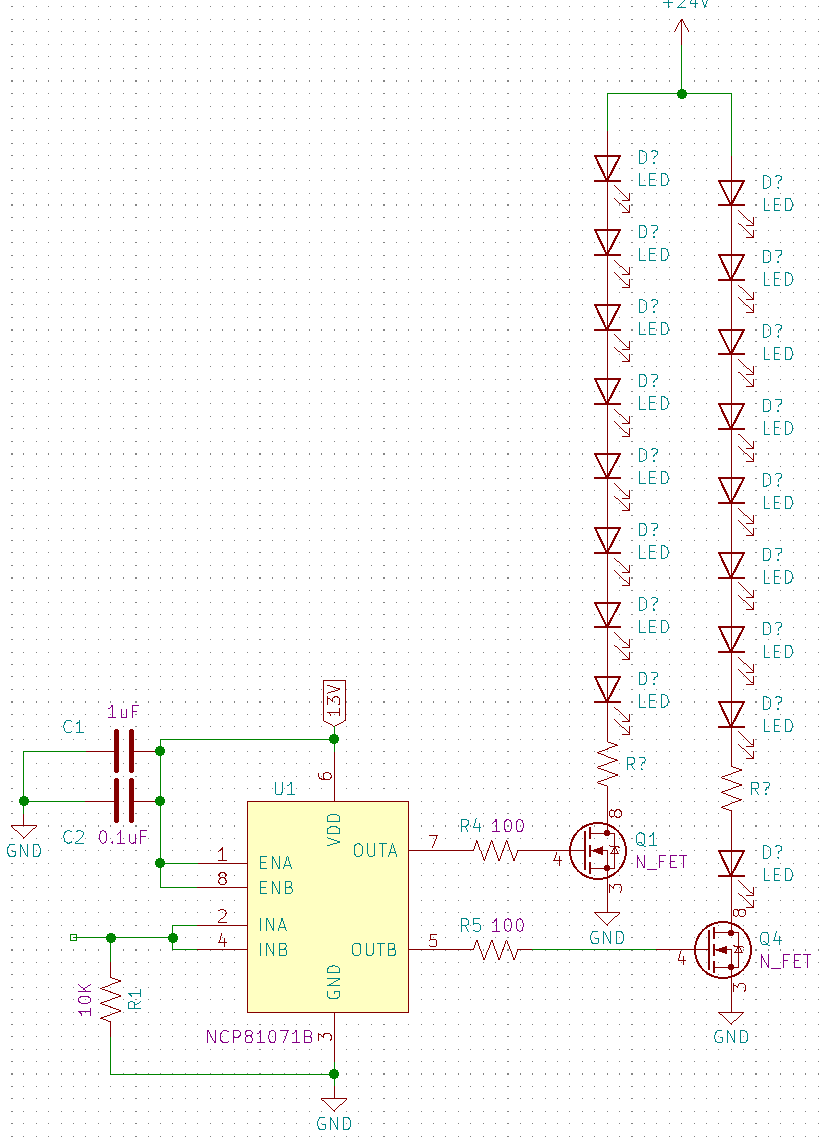
Image 2: A low-side N-channel MOSFET drives each LED strand while a dedicated MOSFET driver switches the MOSFET on/off. This image shows the long strands directly driven by the 24VDC rail.
We then split up the 24V supply rail into three additional rails using switching regulators. We choose 7V, 13V, and 16V. With these specific voltages, we could then drive the rest of the shorter strands the same way as the longer strands, and dissipate the excess power using one or two resistors each. This approach seemed to be the best of both worlds, as we could PWM all of the strands directly, and they would respond the same, while also benefiting from the high efficiency of switching topography.
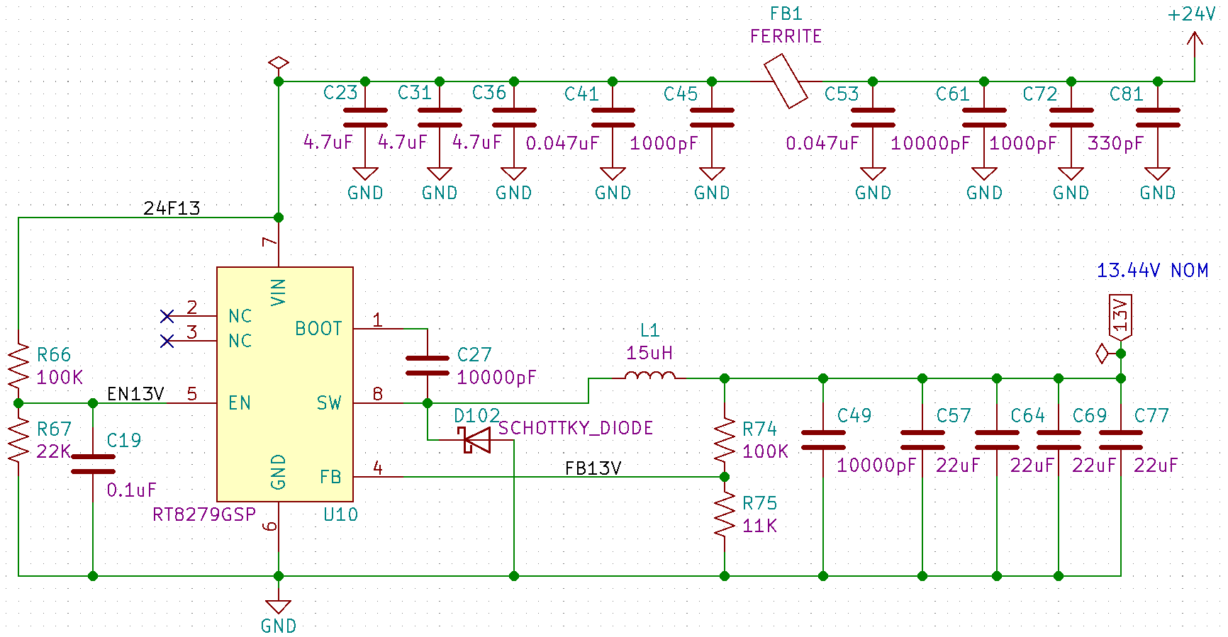
Image 3: A switching regulator – a RT8279 – drops the voltage rails down to a specific voltage, allowing the LEDs to be driven linearly from the new rail.
As shown in image 3, the switching regulator uses a CLC input filter. This filter ensures that high frequency switching noise will not leave the regulator and couple with anything else on the board. There is also a large amount of output capacitance on these rails. This new rail powers the other LEDs that have shorter strands, as shown in image 4.
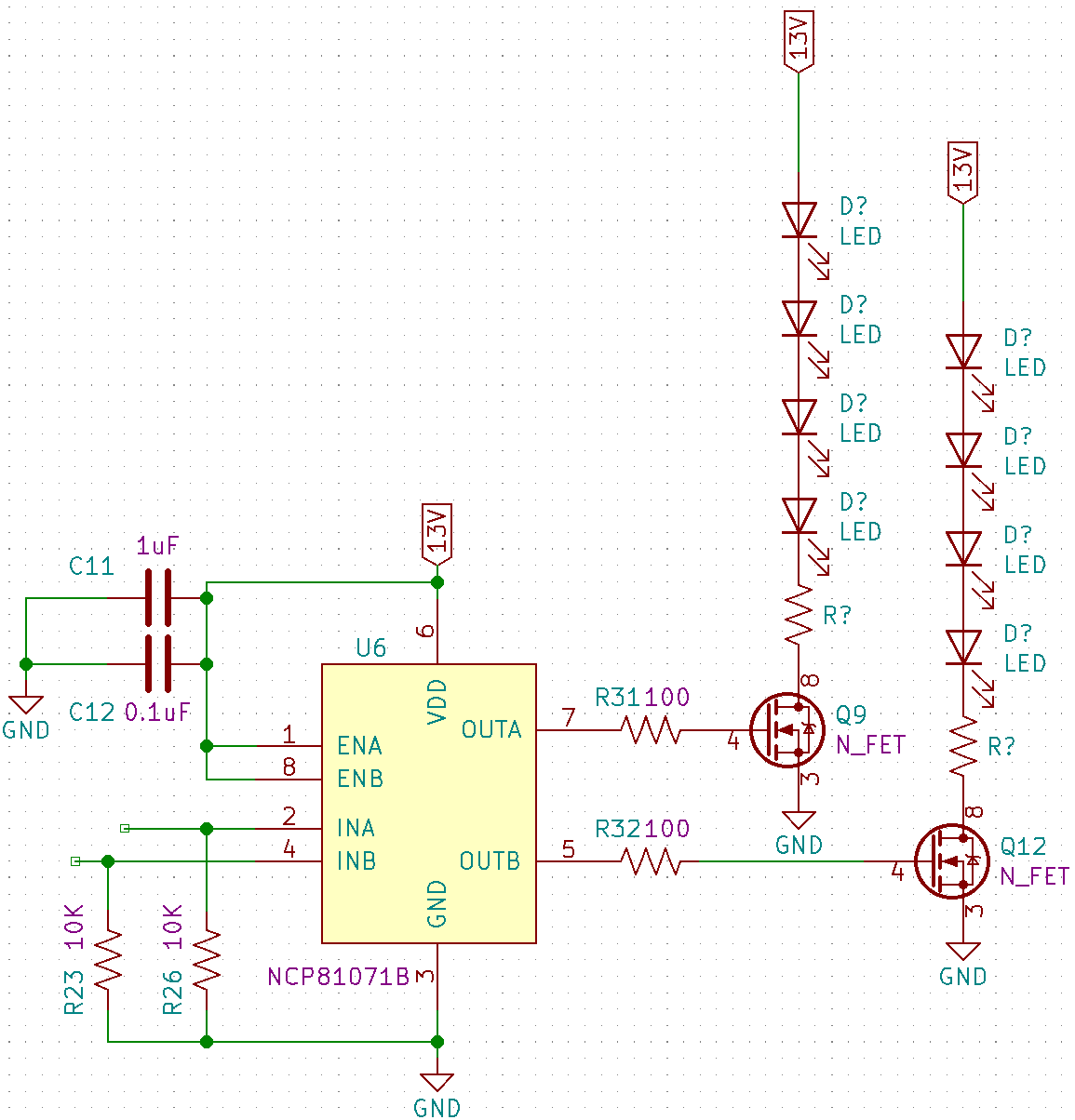
Image 4: The new 13V rail drives the LEDs on the shorter strands. The new voltage rail reduces power losses across the resistors.
Initial Testing
Once the PCB was designed and fabricated and then assembled (which was quite the task in and of itself), it was time to test the board. We started with testing every strand individually at full power. They all functioned as expected. Next, we tested them with a PWM signal – we used 100Hz initially. Starting from around 10% duty cycle with all strands, then slowly increasing. Once at 20%, our power supply started showing all sorts of errors and issues, basically going into overvoltage lockout and then shutting down completely. We then tried at 100% duty cycle and decreased it from there. It worked fine until 80% when the same issue occurred.
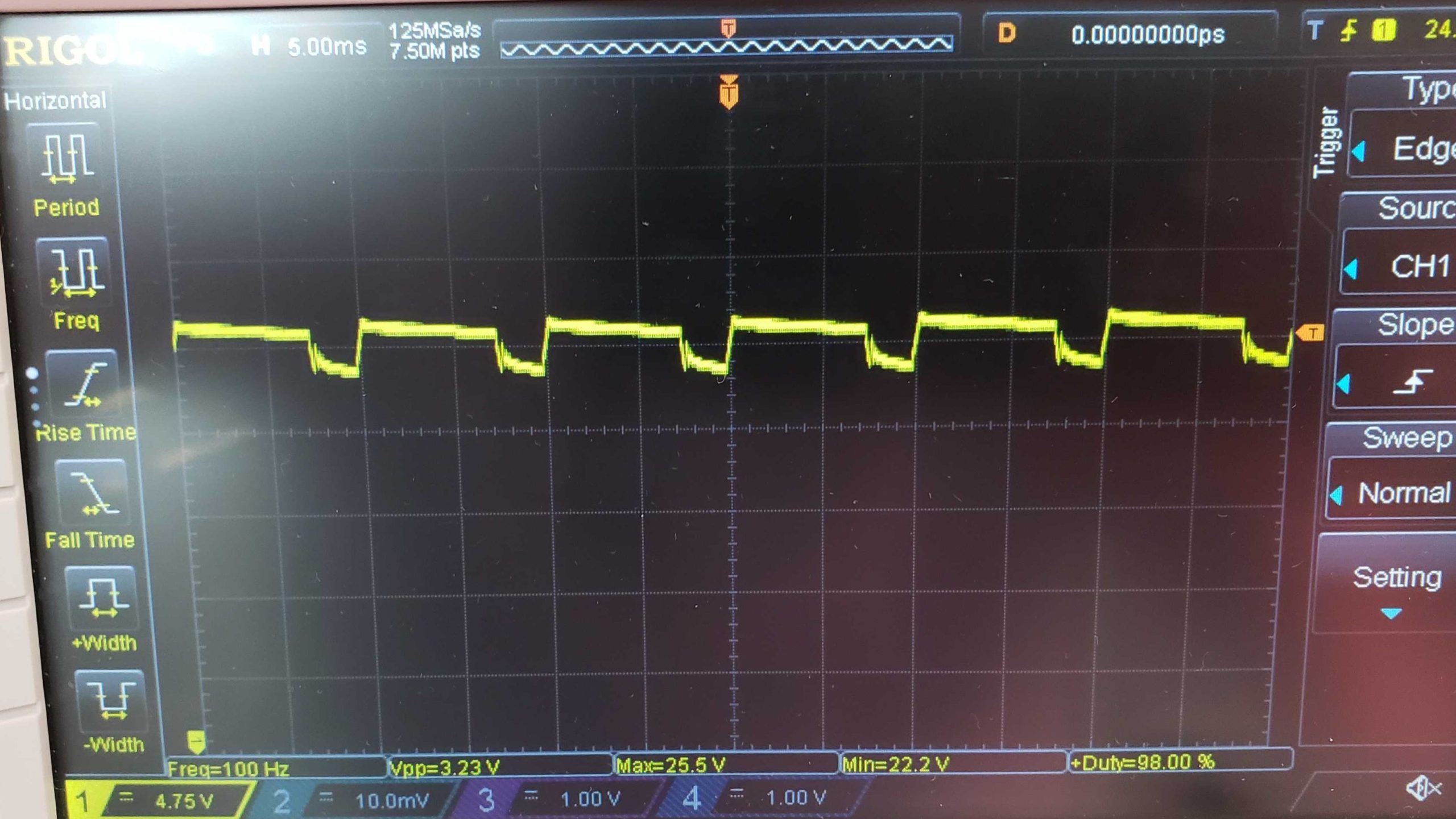
Image 5: When troubleshooting the circuit, the oscilliscope showed a large voltage drop on the same frequancy as the driving PWM signal.
Starting to Troubleshoot the Circuit
There was an issue on the main 24V input rail, so we started our circuit troubleshooting there. We hooked up an oscilloscope to the input terminal of the board. We saw a 3.5V Vpp signal with a sound 100Hz frequency, the same frequency that we were driving the LEDs at (image 5). Every time that the PWM pulse went high, it was dropping the main voltage rail by several volts. The voltage fluctuation explains why the PSU was unhappy.
The next step was to see if we could isolate the issue any more. The majority of the complexity of this design was with the switching regulators. I figured that the strands that were causing the drop were the strands that were going through them. So we turned off all the 24V strands, and only PWM’d the switching regulator powered strands. This nearly eliminated the issue on the rail. There was still a small voltage sag, but not near enough to cause the power supply to complain. Though it was apparent that the native 24V strands were the issue, we still tested them independently. As expected, the scope showed the same massive voltage sag, with the power supply complaining again.
Since we were driving the LEDs with MOSFETs, the instant that the PWM signal went high, there would be a 1A current surge on each of the strands. This is a lot of current for any power rail to supply quickly. The MOSFET drivers that we are using have a 100R resistor between its output and the MOSFET’s gate. Changing this value will slow down or speed up the rate at which the MOSFET will turn on. As a result, this changes how quick the current surge will be. So we changed the values going from 100R up to 1K, then 500K, and even 1M.
While changing the gate resistors did fix the voltage sag issue, it turned on so slowly, that the MOSFET stayed in the linear region the entire time. It essentially acted as a constant current amplifier, instead of a simple on/off switch. When a driving a MOSFET like this, the power losses will be too much to dissipate.
A Possible Solution?
We then decided to look directly into why the strands powered by the other rails weren’t having any issues. Two things immediately jumped out to us: the first is the CLC filter that we placed in front of every regulator, the second is that the output side of the regulator has a lot of capacitance. The CLC filter makes it so that even if the noise were present on these LED strands, it wouldn’t pass through the filter and effect the 24V rail. The bulk capacitance would help prevent the voltage sag from happening in the first place.
The easiest option to test was the capacitance. We put a large 1000uF electrolytic capacitor directly on the main 24V power connector. We then turned on the 24V strands and checked the oscilloscope. Vpp went from 3.5V down to 2.5V, still too much for the power supply, but at least we were going in the right direction! We were too space constrained on the board to use this approach the first however. We wouldn’t be able to fit a single 1000uF capacitor on the board, let alone the potentially required 3 or 4. So even though adding more bulk capacitance appears to be a solution, it isn’t viable for us.
The Actual Solution
I want to say that we constructed a perfect gameplan on how to proceed, but I can’t. We just started trying some different ideas until something happened, which is what troubleshooting circuits often becomes. We changed the PWM frequency to 20kHz, and the voltage drops decreased by over half. The voltage drop was at the same 20kHz drving frequncy. Then we tried 30 kHz, then 50 kHz, and the voltage drops were no longer noticeable on the scope. The power supply didn’t have any issues driving the load anymore. This issue was 100% resolved at all duty cycles, and with all LED strands running. The best solution ended up being a simple software change!
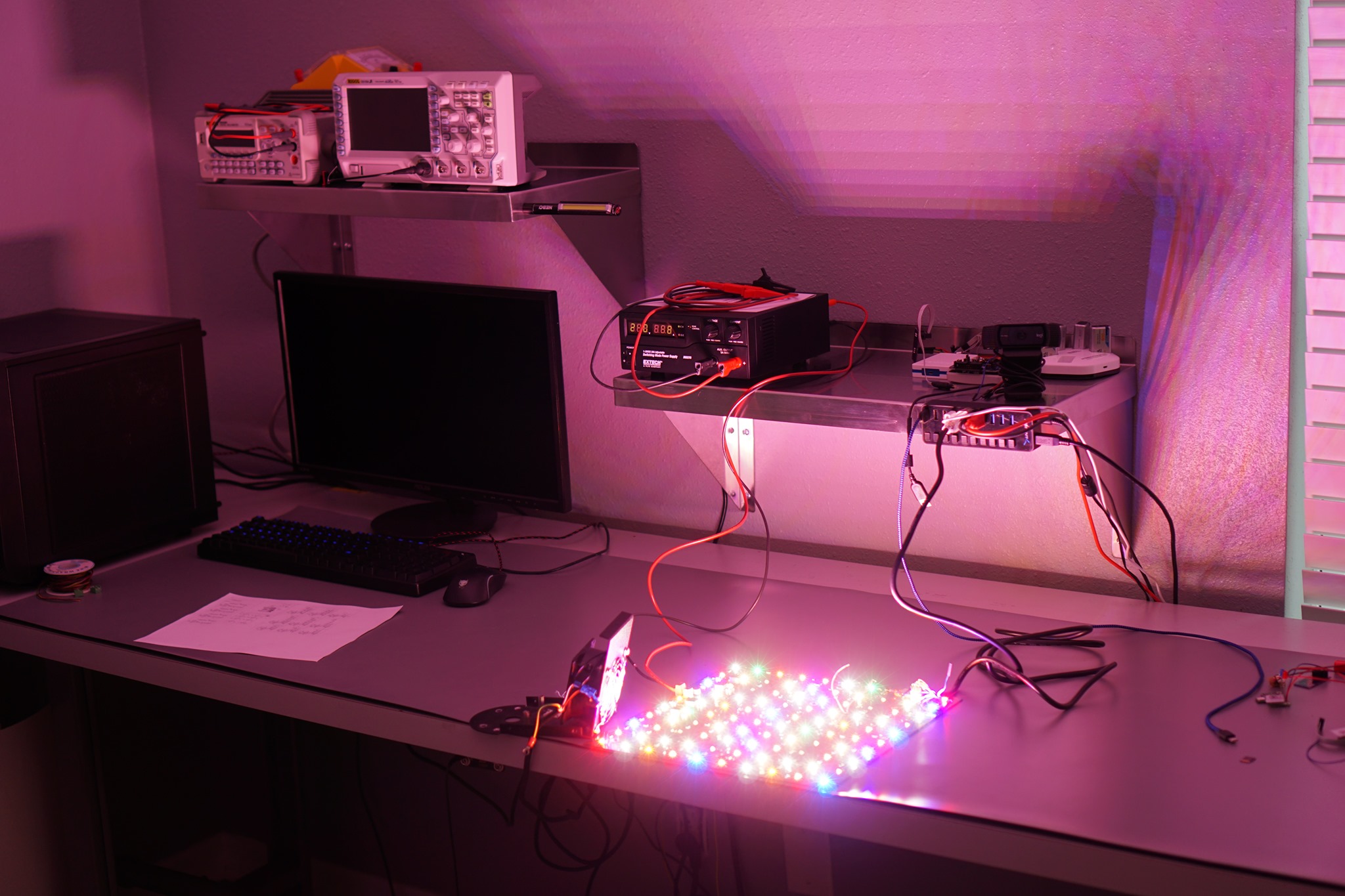
Image 6: After several long days spent troubleshooting, the circuit was finally working as designed!
Solution Explained
Now before I discuss the reasoning behind why merely changing the PWM frequency solved our problem, I must say that this is speculation and best guesses on what we believe. Without doing more in-depth troubleshooting and circuit testing with simulations, we can’t know for 100% that we fully understand the cause.
100Hz Frequency
- Board gets power; input capacitors fully charge up.
- The first PWM signal turns all LEDs on, all at once.
- The current surge drains down the capacitors completely. This forces the board to attempt to source the current from the power supply directly.
- Since there are inductance and resistance on the power supply leads, the PSU is unable to provide the current that the board needs.
- The voltage drops on the board until the supply can “catch up” to the energy demand.
- The PWM cycle turns off; all capacitors can charge up fully.
- Repeat
50kHz Frequency
- Board gets power; input capacitors fully charge up.
- First PWM signal turns all LEDs on, all at once.
- The current surge starts to drain down the capacitors.
- Before the capacitors fully drain down, the PWM cycle turns off, allowing the capacitors to charge back up.
- Repeat
At 100Hz, I am quite confident that my explanation is valid, as there isn’t much else that can explain it. For the 50kHz explanation, I think there may also be an additional factor that is occurring. As previously stated, the wiring in the PSU leads causes resistance and inductance between the PSU and the board. At higher frequency, I believe the magnetic field from the inductance can maintain while sourcing the 10+ amps. The PSU sees a constant 10 amp draw when PWM’d at a high enough frequency. While when at 100Hz, it sees a switched on/off that it is unable to keep up with.
Every circuit that you troubleshoot is going to be different. What is important is having the correct tools and the background knowledge to know where to look for issues. I hope that this article helped show a real-world example of how we were able to solve a seemingly confusing problem with a simple software change.
Well done!
I am curious about the initial choice of 100Hz PWM frequency — why so low? It is interesting that you had to jump up so many orders of magnitude before things smoothed out sufficiently. Were you able to, or did you, do it gradually, or just with a shot in the dark?
A little more explanation of the use and source of the PWM signal would be interesting, particularly in how you modified it to change both the duty cycle and the frequency. I was also curious if there is/was any change in behaviour for a given NCP81071B between those with thee separately driven strands (separate INA and INB frequency and/or duty cycle), vs. those where both strands are driven from the same PWM signal.
Have done any reading on shunt FET dimming for driving strings of LEDs? From what I remember, using a shunt FET rather than having a FET that just opens the circuit during the off part of the cycle, is designed to address the exact problem you’re having.
As a followup, here’s a great paper on the topic: https://www.researchgate.net/publication/340971180_Full-Range_LED_Dimming_Driver_with_Ultrahigh_Frequency_PWM_Shunt_Dimming_Control