While working on my youtube video series, I have had many questions and requests to do a detailed write-up on design considerations for a high powered printed circuit board(PCB). Throughout my career, I have worked on several high powered LED and motor driver boards. The most powerful would peak at around 1000 watts with a 24VDC supply. When researching this project, there wasn’t any information online that discussed proper practices for this type of board. Even more, some sources suggested that 30A should never pass through a PCB at all!
The goal with this article is to discuss some of the methods that I have learned and implemented from these projects and hopefully provide a good starting point for any designer who wishes to design a board that can supply > 30A continuously through a standard PCB.
EXAMPLE HIGH POWER SCHEMATIC
As an example, I will be designing a high powered PCB based on an Atmega328 microcontroller. This board will control two DC motors with an integrated h-bridge driver. Since an h-bridge can also drive pretty much any inductive/resistive load, it can also drive high current LED panels. It will be spec’d to drive a 15A load from each output, for a total of 30A. I will be using KiCad 5.0.2 for this example.
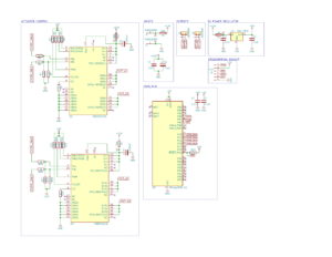
Figure 1: Example Schematic
The schematic in Figure 1 utilizes two VNH5019A integrated h-bridge drivers. They can each drive current of 30A continuously. An Atmega328 will control the logic for the drivers, and a single 12VDC power supply will power the board. A drop in switching regulator will provide the 5VDC supply to the ATmega. The VNH has all logic pulled up, except the Ina/b lines, which provide the direction of rotation for the motor. If more control is required, you can control the ENa/b pins by the ATmega.
The VNH is able to handle most of the flyback protection, only requiring the 1000uF electrolytic capacitors. For more information on protection of circuits from inductive loads, check out my article on the topic: H-Bridge Circuit Basics. I will be using 74651195R 85A Screw terminals for the main 12VDC power inputs, and two 1792229 30A snap terminal blocks for the motor outputs.
There is a 30A input fuse, and a 15A fuse going to each of the VNH drivers. The fuse going to the drivers is before the driver since the driver can supply 30A, the fuse should blow before overloading the driver. This ensures that both sides are cut off when the fuse blows since the driver will have no power at all. Another option would be to fuse both outputs of the H-bridge driver, but this could still leave one side hot after a short.
HIGH CURRENT PCB DESIGN
SAFETY CONSIDERATIONS
As with any circuit, the primary concern with a high current circuit is ensuring that it operates safely. There are a few potential issues that are unique with boards that drive such high powered loads. The main hazard is heat. No matter how well you design and lay out the board, more heat is produced than with a standard board. This must always be considered when the housing is made, and external vents/fans should be used. Something that I do on ALL designs that drive more than a few amps, is to have a dedicated temperature sensor on the PCB. This is a great firmware based failsafe. With the ability to monitor the temperature, you should always be able to react to any situation of overheating. To reduce the amount of heat produced on the board itself, it is best to choose components with low resistance.
The next potential safety hazard is regarding short circuits. Since the board is designed to drive high power devices, when shorted, it will be able to source a considerable amount of current. It is crucial to consider this possibility in the design phase. The easiest way to deal with shorts is to have a fuse on ALL outputs that leave the board, and an input fuse. The fuses should always be rated for less current than the wires used can handle. They also should be rated for less/equal the amount of current the board traces/pours are designed for. It is also a good idea to use drivers that have built-in short circuit prevention built into them.
GET A GAMEPLAN
When planning a high power circuit, before you run the first trace, it is imperative to have a high-level understanding of the layout. While this is important with any board design, it is especially crucial with these boards. While not necessary, I typically like to break boards like this up into low power and high power sections. This ensures that all the high power traces are as close to the power source and outputs as possible. This board will be 2-layers, with 2Oz copper.
Something that I learned while doing high current PCBs, and now do in all of my designs, is to do a rough initial layout with 8 mil traces on everything, to ensure that the placement of components is in an optimized manner. This helps immensely for this example, as it shows where exactly the high current paths will be, and how best to position the H-Bridge drivers.
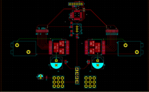
Figure 2: Rough board layout with 8 mil traces.
Figure 2 shows the initial placement of all components, and the 8 mil traces to designate where the paths of all the final traces will be routed. The power will come in from the bottom terminal, head to the input fuse, branch to the H-Bridge drivers, and the low current supply will go up the center of the board to the 5V regulator.
For the H-bridge drivers, power will come to them across the large electrolytic capacitors on the bottom layer, connecting the top layer and pad with many stitching vias.
TRACE WIDTH CALCULATOR
When designing any circuit board, you need to understand the minimum trace width. This becomes crucial when dealing with high powered PCBs. I don’t have a preference to a specific calculator since they are all (should) based on the same IPC-2221 formula. This board has two main high current nets that we will use the calculator. The first is the main 30A supply that comes in from the PSU to the fuse, then branches out. Using a calculator at a 25c temp rise, we need a minimum width of 370mils. The second supply is the 15A that goes from the fuse to the capacitor, then to the drivers. The driver output is rated for the same 15A supply. The calculator recommends a trace width of 142mils.
When designing the board, these values are the absolute minimum widths that should be used.
COPPER POURS ARE YOUR FRIEND
No matter the type of board that I am designing, I always try to use copper pours for all power nets. When dealing with a dedicated high current design, all nets that carry high power should be a pour. Copper pours allow a significant increase in the width of copper that can fit on a board.
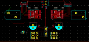
Figure 3: Layout with copper pours used on all high current nets.
Figure 3 shows the high current portion of the board using copper pours on all high current nets. With the pours instead of traces, I am able to expand the amount of copper by a significant amount. A trick that I use to help the design go a bit faster, is to use a 20mil grid and use that to ensure that all of the pours go at 45-degree angles for symmetry.
DOUBLE UP THE LAYERS
One technique that I have used with many high powered circuits that I haven’t seen used often is to have a double layer copper pour and stitch them together with via’s. This double layer allows twice the amount of copper to be within the same area. For this board, I double up the copper on the primary power input from the terminal to the input fuse. Figure 4 shows this. When you use this technique there is an increased chance of creating current loops since you have a section that no return current can flow through. I would not trust using both layers on the net from the input fuse to F3/F4, as that is where a lot of return current will flow.
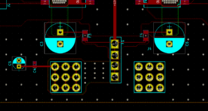
Figure 4: Closeup on the doubled up layers for the primary power input
The minimum width of this pour is 460mils, but since it is on the top and bottom layers, the actual width is double that, allowing for a much smaller voltage drop across the net. The smaller the voltage drop, the less heat that will be produced.
WHAT ABOUT THERMAL RELIEFS
When discussing anything having to do with thermal reliefs in high power PCB design, there is always some disagreement. The purpose of using thermals is preventing heat wicking to the surrounding copper pour when soldering. They work quite well at this. They come at the cost of having less copper for current to flow. For standard PCBs, this tends to be a minor issue, and the benefits of thermals far outweigh the drawbacks. All of the high power PCB designs I have completed, we have hand-soldered them in-house using a high power Hakko Fx-801 iron. It makes quick work of solid pads, even on 2Oz copper. I tend to use thermals on all non-power nets, and solid connections on the power nets.
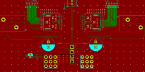
Figure 5: Filled planes showing thermal reliefs
Figure 5 shows where I placed thermal reliefs. The main input supply, fuses, and outputs do not use thermals, with every other net uses thermals. This technique has worked well over several designs, with hundreds of boards produced. We have never had an issue of soldered parts coming loose or any other issue related to having a cold solder joint.
CONCLUSION
Hopefully, this article was able to shed some light on proper techniques and tricks that can be implemented with high powered circuits. While there are many nuances to consider when working on these boards, as long as some basic “rules” are followed, they are not much more complicated than a standard board design. The main keys are to always keep safety in mind, have a solid plan from the start, use as much copper as possible, and always check trace widths with a calculator.
Here at MicroType Engineering, we have years of experience with high-power schematic capture and PCB layout. Contact us to see how we can help assist with your next design!
This is informative for me because in thi post you briefly explain for the tips to high power PCB, we all know PCB is main need of electronics industries. Thank you for this post.
This post briefly explains the tips to high power PCB, which is the main need of electronics industries. Thank you for this post.
Wonderful article. Thank You!
I’m quite new to PCB designing. I always get confused by the mismatch in the trace width suggested by the Calculator and the size of pads in the manufacturer’s footprint of the components. The footprints always seem to have small pad sizes but need wider copper trace for high current. Should I equal the trace width to the diameter of the padding and increase the weight of copper instead? Or is it okay to narrow the copper trace near the component hole? #Through Hole Component #Self Assembly PCB
Yes, that is commonly listed. You can certainly narrow down the trace at the pad. It’s normal to do that when a larger trace is called for.
Glad you enjoyed!